IOUT
mEZDPD1620AS
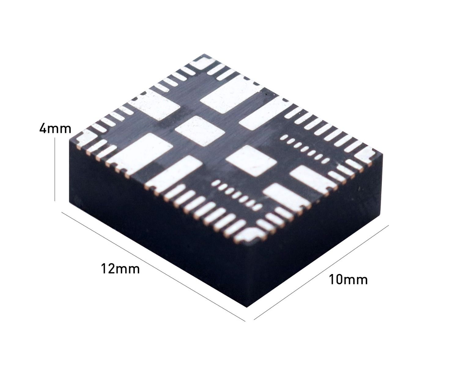
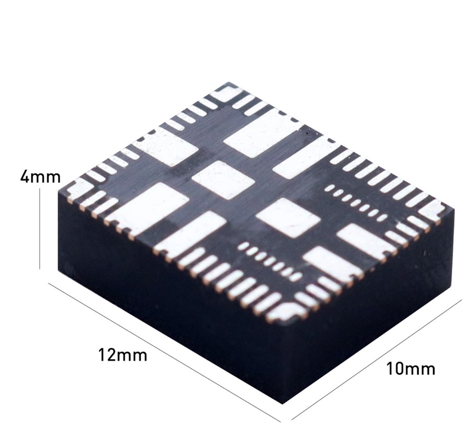
mEZDPD1620AS 是一款可配置的 DC/DC 降压电源模块,可实现高达 25A 的峰值电流和 16V 的输入电压。该模块具有可多次编程的存储器,并可以通过简单的 GUI (图形用户界面) 进行编程。采用简洁的 QFN 封装 (10mmx12mmx4mm)。
Need to configure a different VIN, IOUT?
Session textval
Session Titefor popup
Generating Custom Datasheet
Waveforms of Your Custom Specs
- Start Up
- Steady State
- Load Transient
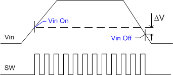
- Vin Shutdown
- Efficiency
- BOM
| 第一步: | 输入定制规格参数并查看定制规格书 |
|
|||||||||||||||||||||||||||||||
|---|---|---|---|---|---|---|---|---|---|---|---|---|---|---|---|---|---|---|---|---|---|---|---|---|---|---|---|---|---|---|---|---|---|
| 第二步: | 保存设计至您的账户 | ||||||||||||||||||||||||||||||||
| 第三步: | 购买您定制的评估板或模块,7天即可交货 | ||||||||||||||||||||||||||||||||
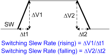
Vo pk-pk: mV @ △Io= A with slew rate 1.6V/us
Target Efficiency: %
Load Current= Efficiency= Power Loss=
Time= Vsw= Vin= Vo= IL= PG= Io=
| Result: | Bandwidth: kHz | Phase Margin: degree |
|
Select a Performance Characteristic to See Results.
| Vin: | V | |
| Io: | A |
| Vin: | V | |
| Io: | A |
| Vin: | V | |
| Io: | A |
| Low Current: | A | |
| High Current: | A | |
| Vin: | V | |
| Vin: | V |
| Low Voltage: | V | |
| High Voltage: | V | |
| Io: | A | |
Notes: For detailed circuit, including the BOM of mEZDPD1620AS, please see the datasheet. Powered by module MPM3596 which includes IC# DIY8886.
Virtual Bench Summary mEZDPD1620AS

 html2canvas
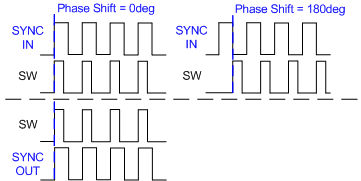
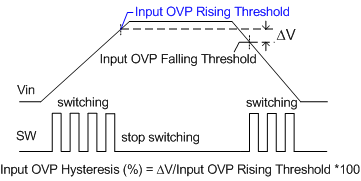
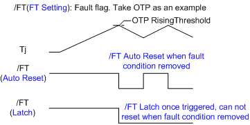
Forced CCM
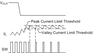
Hiccup
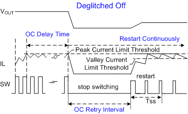
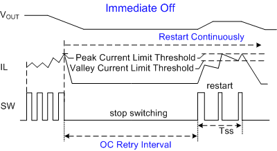
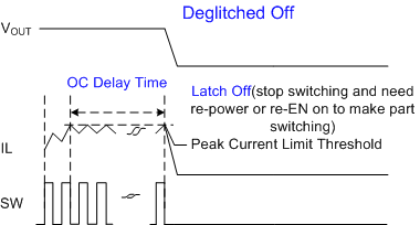
Latch
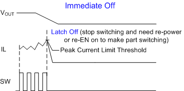
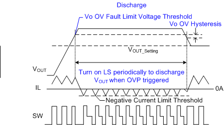
Hiccup
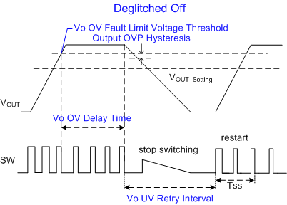
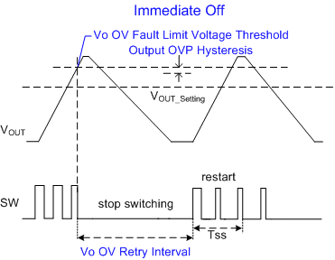
Ignore
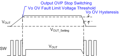
Latch
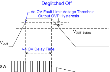
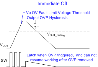
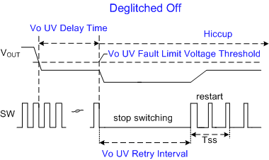
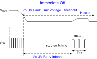
Ignore
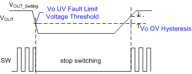
Latch
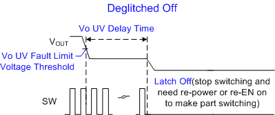
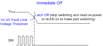

Custom Design
Note: Save design to assign PN
Design Name
PRELIMINARY SPECIFICATIONS SUBJECT TO DESIGN FINALIZATION
DESCRIPTION
This is a fully integrated power module with a PMBus interface. This device offers a complete power solution with excellent load and line regulation over a wide input voltage range. It operates with high efficiency over a wide load range and can be paralleled to deliver a higher load current.
This power module adopts MPS’s proprietary, multi-phase constant-on-time (MCOT) control, which provides ultra-fast transient response and simple loop compensation. The PMBus interface provides module configurations and monitoring of key parameters.
SPECIFICATION OVERVIEW
VOUT
Typical VIN
VIN Min
VIN Max
FEATURES
- Auto-Interleaving for Multi-Phase Operation
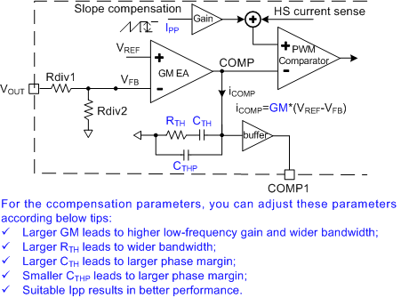
- Auto-Compensation with Adaptive MCOT for Ultra-Fast Transient Response
- 1% Reference Voltage over 0°C to +70°C Junction Temperature Range
- True Remote Sense of Output Voltage
- PMBus 1.3 Compliant
- Telemetry Readback, Including VIN, V>OUTOUT, Temperature, and Faults
- Available in a QFN-59 (10mmx12mmx4mm) Package
EFFICIENCY
VIN = , VOUT = , IOUT =
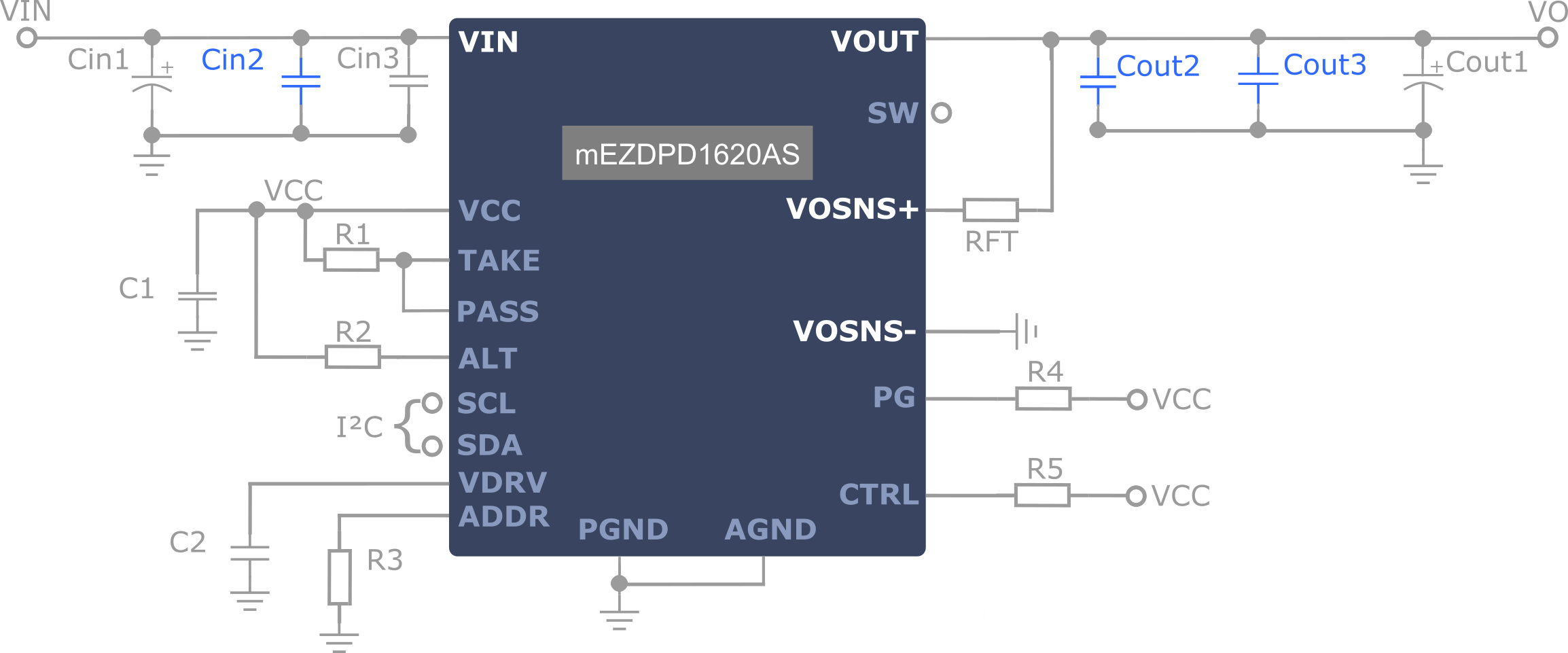
TYPICAL APPLICATION
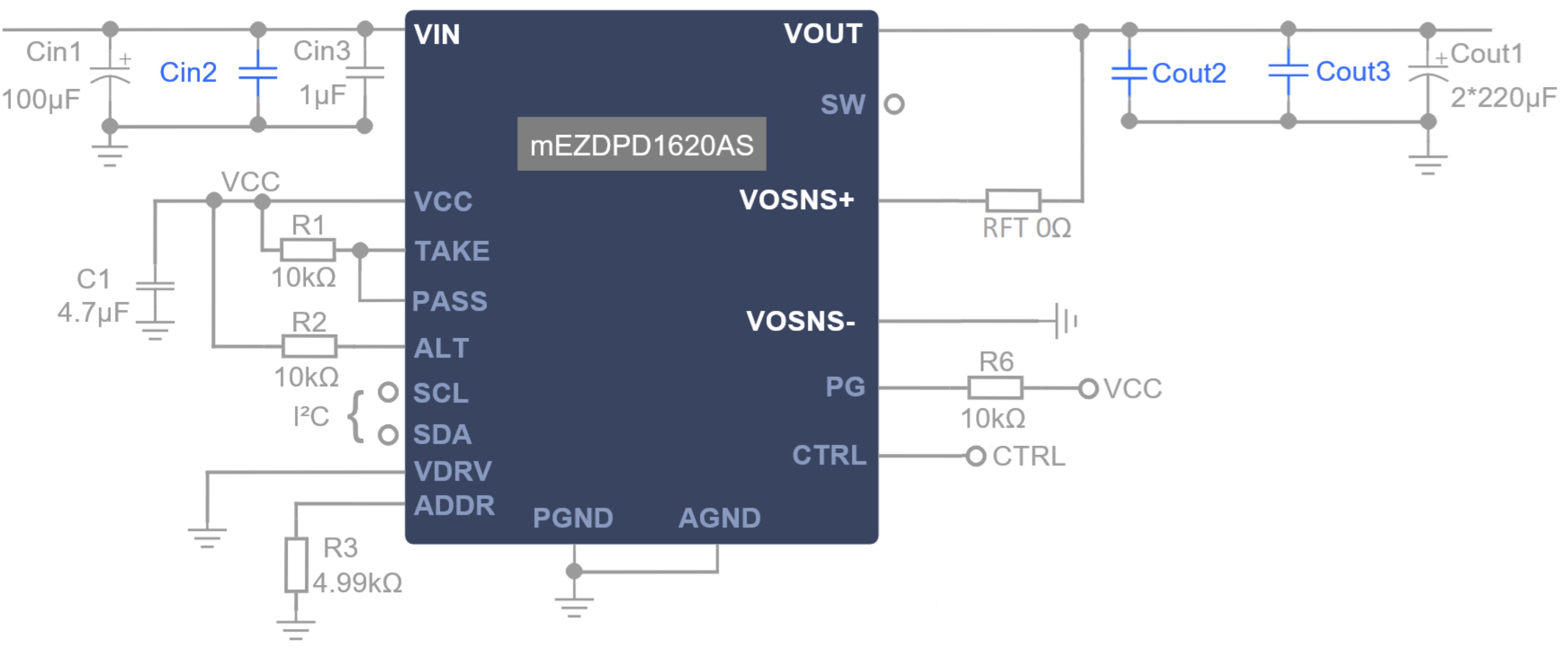
BOM
Reference
Quantity
Value
Description
Package
Manufacturer
Part Number
Cin1
1
100uF
Cap, Electrolytic, 35V
SMD
NIPPON
CHEMI-CON
EMZJ350ADA101MF80G
Cin2
Cin3
1
1uF
Cap, Ceramic, 25V, X7R
'0603'
Murata
GRM188R71E105KA12D
Cout1
2
220uF
Cap, Electrolytic, 6.3V, Tantalum
D2
Panasonic
EEFCX0J221R
Cout2
Cout3
C1
1
4.7uF
Cap, Ceramic, 25V, X7R
'0603'
Murata
GRM188R61E475KE11D
C2
1
4.7uF
Cap, Ceramic, 25V, X7R
'0603'
Murata
GRM188R61E475KE11D
R1
1
10kΩ
Film Res,1%
'0603'
YAGEO
RC0603FR-0710KL
R2
1
10kΩ
Film Res,1%
'0603'
YAGEO
RC0603FR-0710KL
R3
1
4.99kΩ
Film Res,1%
'0603'
YAGEO
RC0603FR-074K99L
R6
1
10kΩ
Film Res,1%
'0603'
YAGEO
RC0603FR-074K99L
RFT
1
0Ω
Film Res,1%
'0603'
YAGEO
RC0603FR-070RL
U1
1
-
Programmable 16V DC/DC Power module supply up to 20A
QFN-59 (10x12x4mm)
MPS
ORDERING INFORMATION
Part Number
Finalize Design to Order
PACKAGE REFERENCE
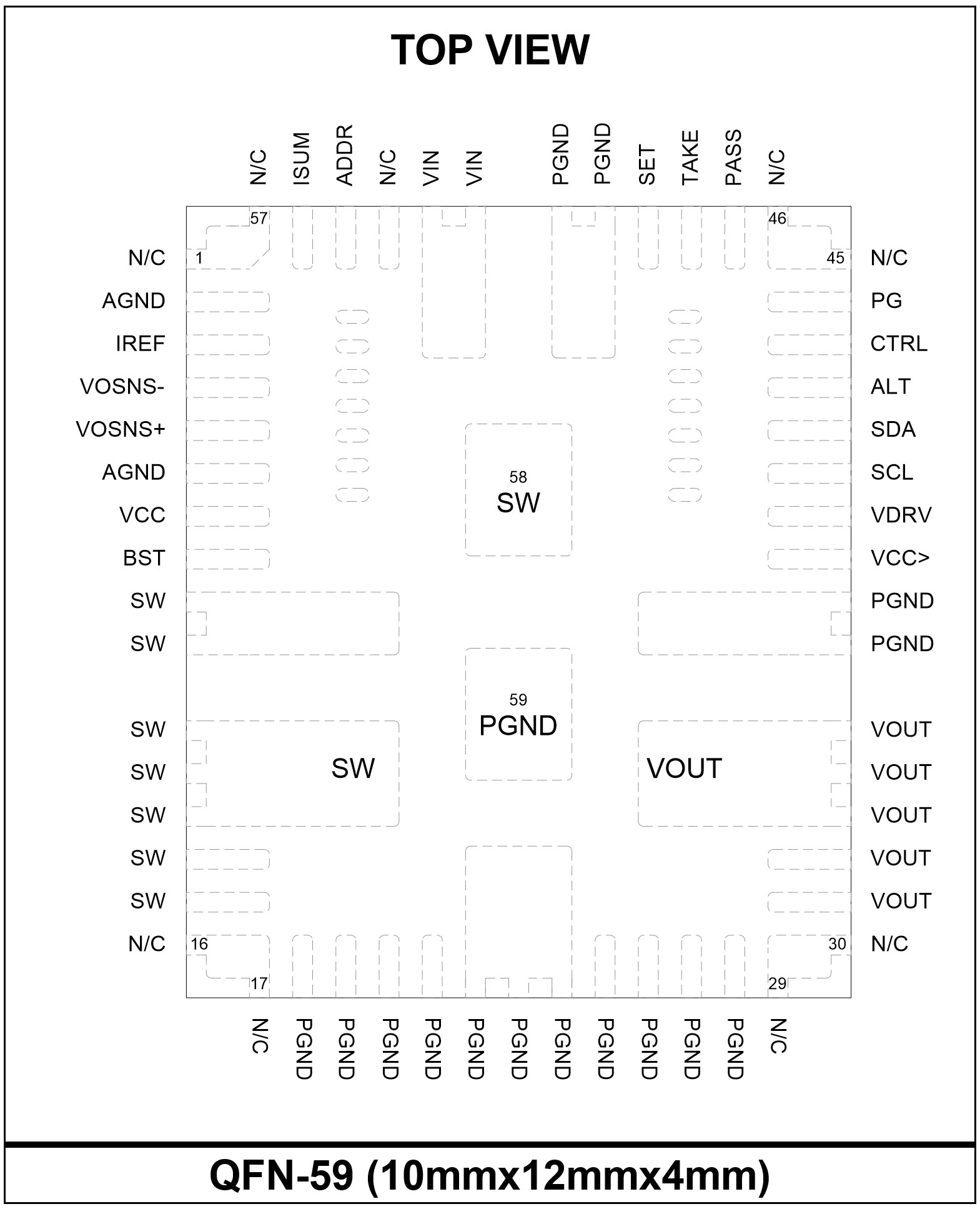
OTHER ORDERING OPTIONS
Evaluation Board for Surface Mount Device
The evaluation board is designed to demonstrate the capabilities of your custom MPS Custom PN.
The EVB device is programmed with custom configuration.
Part Number
EVmEZDPD1620AS-00A
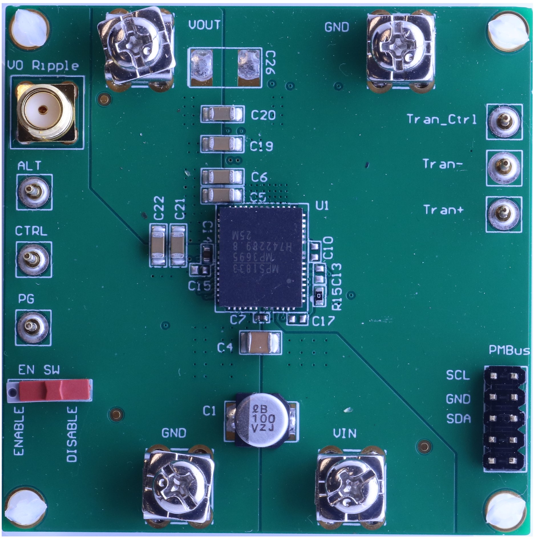
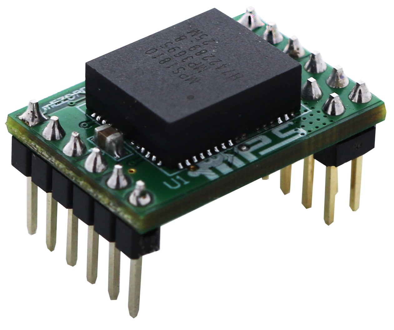
DIP Mount (Pin Out Version)
The Custom PN is your custom device on a DIP mount for an easy-to-use, plug-and-play form factor.
The pin out module device is programmed with custom configuration.
Part Number
mEZDPD1620A
Socket Evaluation Board for DIP Mount
DIP mount socket only. For easy evaluation of pin out module.
Part Number
EVmEZDPD1620A-00A

All EVB schematic and layout files can be found at:
https://www.monolithicpower.com/mezdpd1620as.html
PIN FUNCTIONS
Pin #
Name
Description
2, 6
AGND
Analog ground. Reference point of the control circuit.
3
IREF
Current reference output.Keep this pin floating.
4
VOSNS-
Output voltage sense negative return. Connect directly to the GND sense point of the load. Short to GND if remote sense is not used.
5
VOSNS+
Output voltage sense positive return. Connect this pin to the positive sense point of the output voltage to provide feedback voltage to the system.
7
VCC
Output of the internal 3.3V LDO. The driver and control circuits are powered by this voltage. Must be connected to pin 38.
8
BST
Bootstrap. Keep this pin floating.
9, 10, 11, 12, 13, 14, 15, 58
SW
Switch node. Keep them floating.
31, 32, 33, 34, 35
VOUT
Module output voltage node. Connect with wide PCB copper plane.
18-28, 36, 37, 50, 51, 59
PGND
Power ground. This pin is the reference point of the regulated output voltage. Connect with PCB copper planes as wide as possible.
38
VCC>
Input of driver circuit. Must be connected to pin 7.
39
VDRV
Decoupling pin for 3.3V driver power supply.
40
SCL
PMBus serial clock.
41
SDA
PMBus serial data.
42
ALT
PMBus alert. Open-drain output, active low. A pull-up resistor must be connected to a 3.3V rail.
43
CTRL
Converter control. CTRL is a digital input that turns the regulator on or off. Drive CTRL high to turn the regulator on, drive it low to turn the regulator off. Do not float this pin.
44
PG
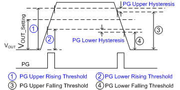
Multi-purpose power good output. This pin can be configured as an output pin for single-phase operation, or as an input and output pin for multi-phase configuration. A pull-up resistor connected to a DC voltage must indicate high if the output voltage exceeds 90% of the nominal voltage. See the Application Information section for detailed configuration.
47
PASS
Passes run signal to the next phase. See the Applications Information section for connection details.
48
TAKE
Receives run signal from the previous phase. See the Typical Application on page 2 for connection details.
49
SET
PWM signal. The set signal turns on the HS-FET when a run signal appears. For multi-phase operation, tie the SET pins of all the phases together.
52, 53
VIN
Supply voltage. This pin provides power to the module. Decoupling capacitors must be connected between VIN and GND. Connect VIN with a wide copper plane.
55
ADDR
PMBus slave address setting pin. Connect a resistor between this pin and AGND to set the address of this device.
56
ISUM
Reference current output. For single-phase operation, keep this pin floating. For multi-phase operation, connect the ISUM pins of all phases together.
1, 16, 17, 29, 30, 45, 46, 54, 57
NC
No internal connection.
ABSOLUTE MAXIMUM RATINGS
(1)Supply voltage (VIN)
18V
VSW (DC)
-0.3V to VIN+0.3V
VSW (25ns) (2)
-3V to +25V
VSW (25ns)
-5V to +25V
VOUT
5.5V
VBST
VSW +4V
VCC
4.5V
CTRL current (ICTRL)
2.5mA
All other pins
-0.3V to +4.3V
Continuous power dissipation (TA = 25°C) (3)
5 W
Junction temperature
170°C
Lead temperature
260°C
Storage temperature
-65°C to +170°C
Supply voltage (VIN)
4V to 16V
Output voltage (VOUT)
0.5V to 5.5V
External VCC bias
3.12V to 3.6V
CTRL current (ICTRL)
1mA
Operationg junction temp (TJ)
-40°C to +125°C
Thermal Resistance (5)
θJA
θJC
QFN-59 (10x12x4mm)
17 °C/W
3.4 °C/W
- 1) Exceeding these ratings may damage the device.
- 2) Measured by using differential oscilloscope probe
- 3) The maximum allowable power dissipation is a function of the maximum junction temperature TJ (MAX), the junction-to-ambient thermal resistance θJA, and the ambient temperature TA. The maximum allowable continuous power dissipation at any ambient temperature is calculated by PD (MAX) = (TJ (MAX) - TA) / θJA. Exceeding the maximum allowable power dissipation produces an excessive die temperature, causing the regulator to go into thermal shutdown. Internal thermal shutdown circuitry protects the device from permanent damage.
- 4) The device is not guaranteed to function outside of its operating conditions.
- 5) Measured on EVM3695-25-RF-02A, 6-layer demo board PCB.
PROGRAMMABLE ELECTRICAL CHARACTERISTICS
Parameter
Symbol
Description
Min
Typ
Max
Units
Input Voltage
Input voltage range
VIN
Programmed value
V
Input over-voltage fault limit
Programmed value
V
Input over-voltage warning limit
Programmed value
V
Input voltage under-voltage warning limit
Programmed value
V
Output Voltage
VOUT command (6)
VOUT
Programmed value
V
Output voltage scale
VOUT SCALE
Programmed value
Output voltage margin high
VOUT_MARGIN_HIGH
Programmed value
V
Output voltage margin low
VOUT_MARGIN_LOW
Programmed value
V
Output voltage min
VOUT MIN
Programmed value
V
Output voltage max
VOUT MAX
Programmed value
V
Output voltage step
VOUT_STEP
Programmed value
V
Current Limit
Valley current limit
ILIM_VALLEY
Programmed value
A
Min valley current limit programmable value (6)
ILIM_VALLEY_MIN
Programmed value
A
Max current limit programmable value (6)
ILIM_VALLEY_MAX
Programmed value
A
Low-side negative current limit in OVP
ILIM_NEG_OVP
Programmed value
A
Delay time after low-side negative current limit in OVP
tDEALY_NOCP
Programmed value
ns
Output current limit (DC)
ILIM_DC
Programmed value
A
Output over-current warning (DC)
IWARN_DC
Programmed value
A
Over-current fault hiccup interval time
tITV_HICCUP
Programmed value
ms
Frequency
Switching frequency
fSW
Programmed value
KHz
Output Over-Voltage and Under-Voltage Protection
OVP threshold
VOVP
Programmed value
VREF
UVP threshold
VUVP
Programmed value
VREF
Soft Start and Turn On/Off Delay
Soft-start time
tSS
Programmed value
ms
Turn-on delay (6)
tON_DELAY
Programmed value
ms
Turn-off delay
tOFF_DELAY
Programmed value
ms
Output Under-Voltage Lockout (UVLO)
Input programmable turn-on voltage
VIN_ON
Programmed value
V
Input programmable turn-off voltage
VIN_OFF
Programmed value
V
Min input programmable turn-on voltage
VIN_ON_MIN
Programmed value
V
Max input programmable turn-on voltage
VIN_ON_MAX
Programmed value
V
Min input programmable turn-off voltage
VIN_OFF_MIN
Programmed value
V
Max input programmable turn-off voltage
VIN_OFF_MAX
Programmed value
V
Power Good
Power good high threshold, PG_ON
PGVth-Hi
Programmed value
VREF
Power good low threshold, PG_OFF
PGVth-Lo
Programmed value
VREF
Power good low-to-high delay, PG delay
PGTd
Programmed value
ms
Thermal Protection (TP)
TP fault rising threshold (6)
TSD_RISE
Programmed value
°C
TP warning rising threshold (6)
TWARN_RISE
Programmed value
°C
TP hysteresis
Programmed value
°C
Compensation
Ramp
Programmed value
mV
PROGRAM OPERATION SETTINGS
Name
Selected Mode
Description
Note
Output Voltage
Output voltage discharge
0: No active
1: At CTRL low
Output voltage range
Chooses the internal voltage divider ratio.
00: External divider (0.5~0.672V)
01: Internal divider2:1 (0.5~1.344V)
10: Internal divider4:1 (0.7~2.688V)
11: Internal divider8:1 (1.3~5.376V)
Light-Load Operation Mode
Skip CCM (SYNC)
0: Pulse skip mode
1: Forced CCM
Protection Response
Over-current response
0: Latch-off
1: Retry
Output over-voltage response
0: Latch-off with output discharge
1: Latch-off without output discharge
2: HICCUP with output discharge
3: HICCUP without output discharge
TP response
0: Latch-off
1: Retry
Compensation
Slave Fault Detection
Enable or disable the slave fault detection function through the PG pin.
0: Enable
1: Disable
Operation
Operation
Operation is a paged register. The operation command turns the converter output on/off in conjunction with input from the CTRL pin. It also sets the output voltage to the upper or lower MARGIN voltages.
0: On
1: Soft off
2: Immediate off
3: Margin low (ignore fault)
4: Margin low (act on fault)
5: Margin high (ignore fault)
6: Margin high (act on fault)
On/Off Configuration
PON
0: Enable converter (converter powers up any time the input voltage is present regardless of the state of the CTRL pin)
1: Disable converter (converter does not power up until commanded by the CTRL pin and operation command)
OP
0: Ignore (converter ignores the “on” bit in the operation command from the PMBus)
1: Response (converter responses the “on” bit in the operation command from the PMBus)
EN
0: Ignore CTRL pin (on/off controlled only by the operation command)
1: Require CTRL pin
POL
0: Active low (Pull the CTRL pin low to start the converter)
1: Active high (Pull the CTRL pin high to start the converter)
Write Protect
Write protect
Controls writing to the converter.
0: Enable all
1: Disable function 1 (disable all writes except to the WRITE_PROTECT, OPERATION, PAGE, ON_OFF_CONFIG and VOUT_COMMAND commands)
2: Disable function 2 (disable all writes except to the WRITE_PROTECT, OPERATION and PAGE commands)
3: Disable function 3 (disable all writes except to the WRITE_PROTECT command)
Address PMBus
Enable
Address selection method
0: The address is decided by the ADDR pin
1: The address is decided by MFR_ADDR_PMBUS
Address
Device Address
ADDR
Extra Functions
Total OC hiccup interval
0: Fixed OCP hiccup interval
1: Adjustable OCP hiccup
OSM
0: Enable OSM (output sink mode)
1: Disable OSM
Phase operation
0: For single-phase operation
1: For multi-phase operation
ELECTRICAL CHARACTERISTICS
VIN = 12V, VEN = 2V, TA= -40°C to +125°C, typical values refer to TJ = 25°C, unless otherwise noted.
Parameter
Symbol
Condition
Min
Typ
Max
Units
Vin Supply Current
Supply current (shutdown)
IIN
VCTRL = 0V
2.5
4
mA
Output Voltage
Load regulation (6)
VOUT_DC_LOAD
IOUT from 0A to 25A
±0.5
%VOUT
Line regulation (6)
VOUT_DC_LINE
VIN from 4V to 16V, IOUT = 20A
±0.5
%VOUT
CTRL
CTRL on threshold
CTRLON
2.04
2.2
V
CTRL off threshold
CTRLOFF
1.66
V
Frequency and Timer
Minimum on time (6)
tON_MIN
fSW = 1000kHz, VO = 0.6V
50
ns
Minimum off time (6)
tOFF_MIN
VFB = 580mV
220
ns
Output Over-Voltage and Under-Voltage Protection
OSM threshold rising
VOSM_RISE
104%
VREF
OSM threshold failing
VOSM_FALL
102%
VREF
ADC (6)
Voltage Range
0
1.28
V
ADV resolution
10
Bits
DNL
1
LSB
Sample rate
3
kHz
DAC (Feedback Voltage)
Range
500
600
672
mV
Feedback accuracy
VFB
TJ = 25°C
594
600
606
mV
Feedback accuracy
VFB
TJ = -40°C to +125°C
591
600
609
mV
Resolution (6)
Per LSB
2
mV
Feedback voltage with margin high (6)
VFB_MG_HIGH
672
mV
Feedback voltage with margin low (6)
VFB_MG_LOW
500
mV
Error Amplifier
Feedback current
IFB
VFB = VREF
50
100
nA
Soft Shutdown
Soft shutdown discharge FET
RON_DISCH
60
Ω
Under-Voltage Lockout (UVLO)
VCC under-voltage lockout threshold rising
VCCVth
Default setting
2.6
2.75
2.9
V
VCC under-voltage lockout threshold hysteresis
VCCHYS
Default setting
200
Default setting
mV
Power Good
Power good sink current capability
VPG
IPG = 10mA
0.3
V
Power good leakage current
IPG_LEAK
VPG = 3V
1.5
µA
Power good low-level output voltage
VOL_100
VIN = 0V, pull PGOOD up to 3.3V through a 100kΩ resistor, TJ = 25°C
600
720
mV
VOL_10
VIN = 0V, pull PGOOD up to 3.3V through a 10kΩ resistor, TJ = 25°C
700
820
Monitoring Parameters
Output voltage monitor accuracy
MVOUT_ACC
VO = 0.6V
-2%
0.6
2%
V
Output voltage bit resolution
1.5
mV
Output current monitor accuracy (6)
MIOUT_ACC
VO = 1.2V, fSW = 600kHz, IO = 20A
-10%
20
10%
mV
Output current bit resolution (6)
62.5
mA
Input voltage monitor accuracy
MIN_ACC
-2%
12
2%
V
Input voltage bit resolution (7)
25
mV
PMBus DC Characteristics (SDA, SCL, ALERT) (6)
Input high voltage
VIH
2.1
V
Input low voltage
VIL
0.8
V
Output low voltage
VOL
IOL = 1mA
0.4
V
Input leakage current
ILEAK
SDA, SCL, ALERT = 3.3V
-10
10
µA
Maximum voltage (SDA, SCL, ALERT, CTRL)
VMAX
Transient voltage including ringing
-0.3
3.3
3.6
V
Pin capacitance on SDA,SCL
CPIN
10
pF
PMBus Timing Characteristics (7)
Min operating frequency
10
kHz
Max operating frequency
1000
kHz
Bus free time
Between stop and start conditions
4.7
µs
Holding time
4.0
µs
Repeated start condition set-up time
4.7
µs
Stop condition set-up time
4.0
µs
Data hold time
300
ns
Data set-up time
250
ns
Clock low time out
25
35
ms
Clock low period
4.7
µs
Clock high period
4.0
50
µs
Clock/data fall time
300
µs
Clock/data rise time
1000
µs
Note:
6) Guaranteed by design, not tested in production. The parameter is tested during parameters characterization.
7) Typical Performance Characteristics
TYPICAL PERFORMANCE CHARACTERISTICS
All waveforms simulated.
EFFICIENCY
VIN = , VOUT = , IOUT =
START-UP
VIN = , IOUT =
VIN SHUTDOWN
VIN = , IOUT =
STEADY STATE RIPPLE
VIN = , IOUT =
LOAD TRANSIENT
VIN = , IHIGH = , ILOW = , Slew Rate =
FUNCTIONAL BLOCK DIAGRAM
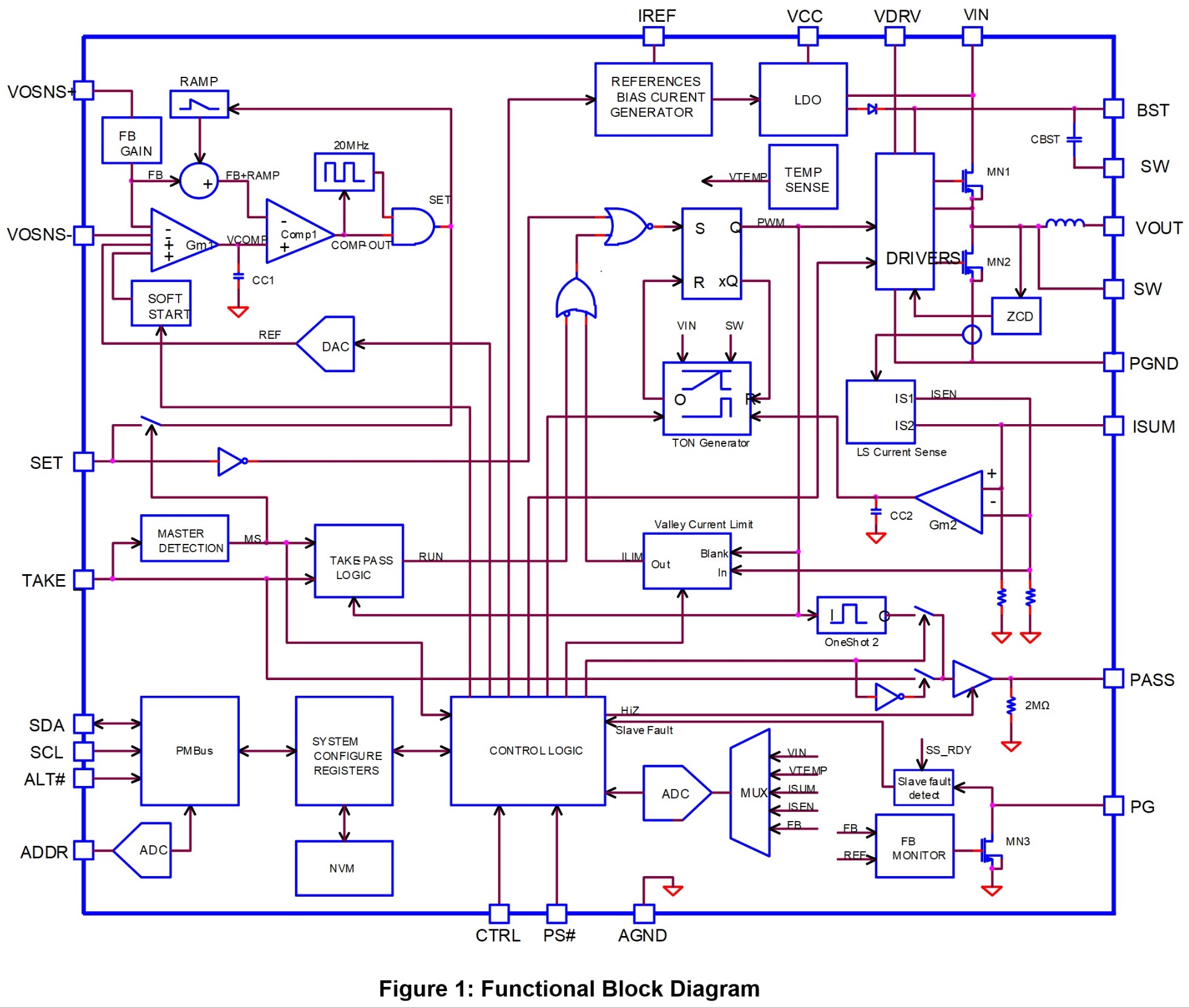
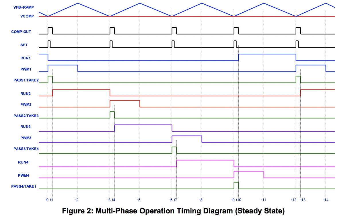
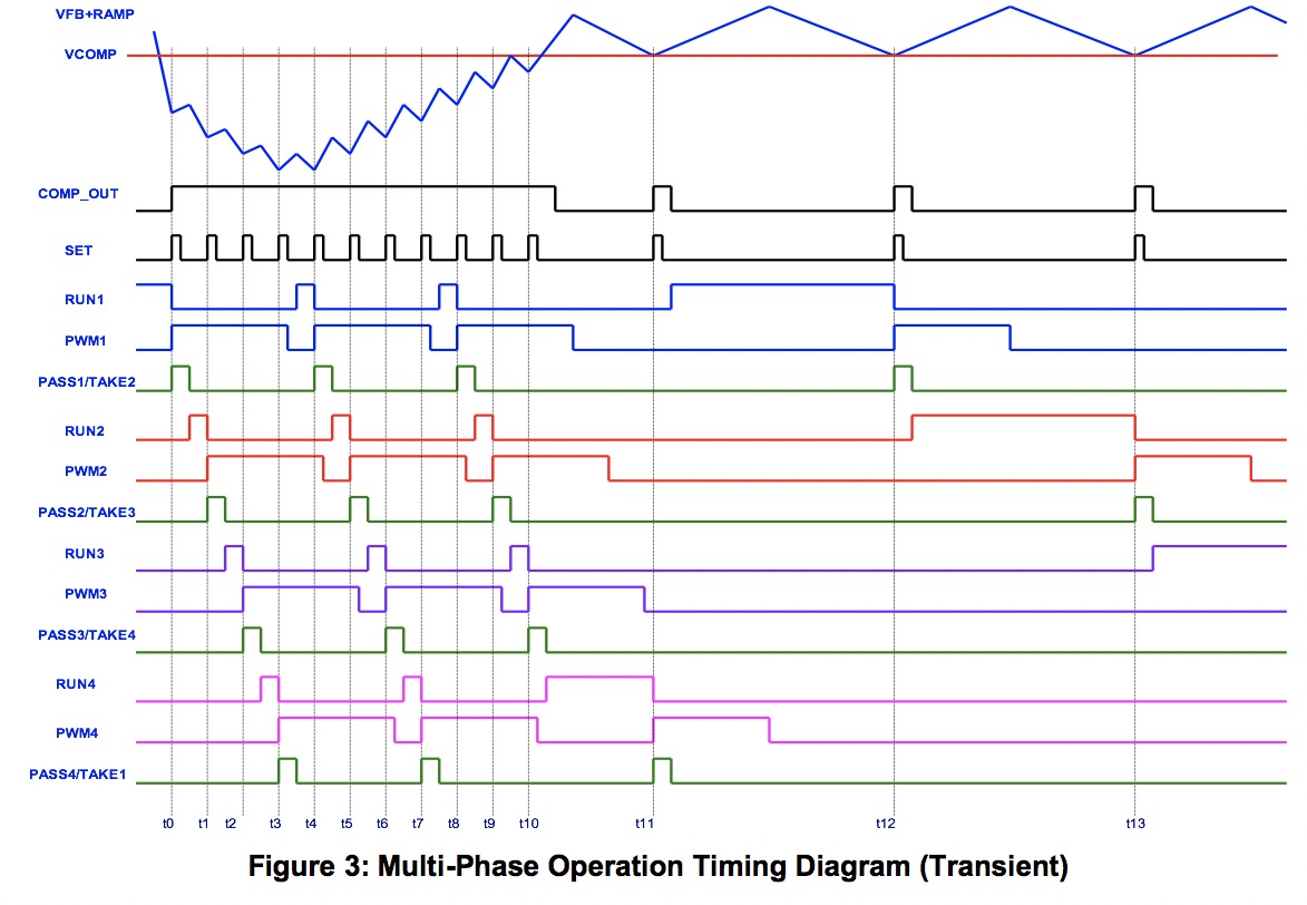
OPERATION
This device is a fully integrated power solution in a QFN-59 (10mmx12mmx4mm) package. For higher current applications, this device can be connected in parallel to provide a higher output current. This device employs constant-on-time (COT) control to provide fast transient response. The internal ramp compensation guarantees stable operation for applications using zero-ESR ceramic output capacitors.
RAMP Compensation
This device guarantees stable operation with zero-ESR ceramic output capacitors by using internal ramp compensation. A triangular RAMP signal is generated internally and superimposed onto the FB signal. The triangular RAMP signal starts to rise once RAMP + FB drops below the REF signal, and a SET pulse is generated. The RAMP signal’s rise time is fixed. The amplitude of the ramp compensation is selectable through the PMBus command D0h[3:1] to support wide operation configurations.
There is a tradeoff between the stability and load transient response. A larger RAMP signal provides higher stability but a slower load transient response, and vice versa. Consequently, it is necessary to optimize the ramp compensation selection based on the design criteria for each application.
APPLICATION INFORMATION
Operation Mode Selection
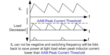
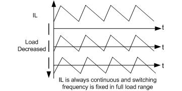
This device provides both forced CCM and pulse skip operations in light-load conditions.
Output Voltage Setting
A feedback resistor divider is required to set the proper feedback gain. The values of the feedback resistors are determined using Equation (1):

Where V0 is the output voltage.
The output voltage feedback gain is determined with Equation (2):

To optimize the load transient response, a feed-forward capacitor (CFF) must be placed in parallel with R1. Table 1 lists the values of the feedback resistors and the feed-forward capacitor for common output voltages.
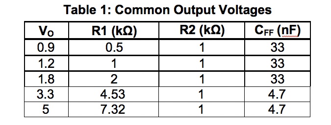
This device offers output voltage programmability through the PMBus. In addition, the output voltage can be adjusted within a certain range through the PMBus by adjusting the internal reference voltage of the PWM controller (VREF). The reference voltage, which has a default value of 0.6V, can be adjusted between 0.5V and 0.672V. For a given feedback resistor network, the upper and lower limits of the output voltage are determined with Equation (3) and Equation (4), respectively:
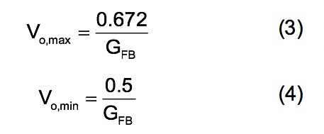
Two steps must be followed to program the output voltage through the PMBus:
1. Write the GFB value determined by Equation (2) to register VOUT_SCALE_LOOP (29h).
2. Write the output voltage command to register VOUT_COMMAND (21h).
VREF is updated automatically based on the output voltage command and GFB.
Output voltage monitoring through the PMBus is enabled by setting the register VOUT_SCALE_LOOP (29h) with a value that matches the GFB value calculated with Equation (2).
For applications where a PMBus interface is not required, VREF = 0.6V is used by default, and operates in analog mode. The feedback resistors should be determined based on Equation (1).
Soft Start
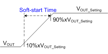
The soft-start (SS) time can be programmed through the PMBus.
Pre-Bias Start-Up
The device is designed for monotonic start-up into pre-biased loads. If the output voltage is pre-biased to a certain voltage during start-up, both the high-side and low-side switches are disabled until the internal reference voltage exceeds the sensed output voltage at the FB pin.
Output Voltage Discharge
The output voltage discharge mode is enabled when the device is disabled through the CTRL pin. In this case, both the high-side and low-side switches are latched off. A discharge FET connected between SW and GND turns on to discharge the output capacitor. A typical on resistance for the discharge FET is about 60Ω. Once the FB voltage drops below 10% of the reference output voltage, the discharge FET turns off.
This feature can be enabled or disabled through the MFR_CTRL_VOUT (D1h) command.
Current Sense and Over-Current Protection (OCP)
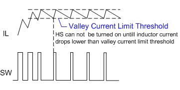
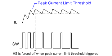
This device features on-die current sense and a programmable positive current limit threshold. The device provides both inductor valley current limits (set by register D7h).
Inductor Valley Over-Current Protection (D7h)
During the LS-FET on state, the inductor current is sensed and monitored cycle by cycle. The HS-FET is only allowed to turn on if no over-current (OC) is detected during the LS-FET on state. If 31 consecutive cycles of an OC condition are detected, OCP is triggered.
During an over-current condition or output short circuit condition, if the output voltage drops below the under-voltage protection (UVP) threshold, the device enters OCP immediately.
Once OCP is triggered, the device either enters hiccup mode or latch-off mode, depending on the register. VCC or CTRL must be power recycled to re-enable the device once it latches off.
The inductor valley over-current limit can be programmed through register D7h, which sets the per-phase inductor valley current limit for both single-phase and multi-phase operation.
Negative Inductor Current Limit
When the LS-FET detects a negative current below the limit set through register D5h[2], the part turns off its LS-FET for a period of time to limit the negative current. The period is set through register D5h[3].
Under-Voltage Protection (UVP)
The device monitors the output voltage through the FB pin to detect an under-voltage condition. If the FB voltage drops below the UVP threshold (set through register VOUT_UV_FAULT_LIMIT), the UVP is triggered. After UVP is triggered, the device enters either hiccup mode or latch-off mode, depending on the PMBus selection. VCC or CTRL must be power recycled to re-enable the device once it latches off.
Over-Voltage Protection (OVP)
The device monitors the output voltage using the FB pin connected to the tap of a resistor divider to detect an over-voltage condition. See the register VOUT_OV_FAULT_RESPONSE section on page 31 for additional information on OVP.
Output Sinking Mode (OSM)
The device enters OSM when the output voltage is more than 5% above the reference and below the OVP threshold. Once OSM is triggered, the device runs in forced CCM. The device exits OSM when the HS-FET turns back on.
Over-Temperature Protection (OTP)
The device monitors the junction temperature. If the junction temperature exceeds the threshold value (set by register OT_FAULT_LIMIT), the converter enters either hiccup mode or latch-off mode, depending on the PMBus selection. VCC or CTRL must be power recycled to re-enable the device once it latches off.
Power Good (PG)
The device has an open-drain power good (PG) output. The PG pin can be configured as output-only or as an input and output pin by bit[0] of register MRF_CTRL_COMP (D0h).
For single-phase configuration, the PG pin should be configured as output-only.
For multi-phase operation, the PG pin should be configured as an input and output pin to detect faults from the slave phases. The PG pin must be pulled high to V¬¬CC or a voltage source with less than 3.6V through a pull-up resistor (typically 100kΩ).
PG is pulled low initially once input voltage is applied to the device. After the FB voltage reaches the threshold set by register POWER_GOOD_ON, the PG pin is pulled high after a delay set by register MFR_CTRL_VOUT.
PG latches low if any fault occurs, and the relevant protection feature is triggered (e.g. UV, OV, OT, UVLO, etc.). After PG latches low, it cannot be pulled high again until a new soft start is initialized.
If the input supply fails to power the device, PG latches low. Figure 4 shows the relationship between the PG voltage and the pull-up current.
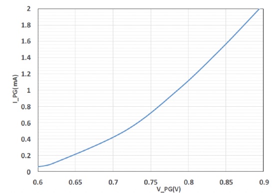
Figure 4: Power Good Current vs. Power Good Voltage
Input Capacitor
The step-down converter has a discontinuous input current, and requires a capacitor to supply the AC current to the device while maintaining the DC input voltage. Use ceramic capacitors for the best performance. During layout, place the input capacitors as close to the IN pin as possible.
The capacitance can vary significantly with temperature. Capacitors with X5R and X7R ceramic dielectrics are recommended because they are fairly stable over a wide temperature range.
The capacitors must also have a ripple current rating that exceeds the converter’s maximum input ripple current. Estimate the input ripple current using Equation (5):

The worst-case condition occurs at VIN = 2VOUT, calculated with Equation (6):

For simplification, choose an input capacitor with an RMS current rating that exceeds half the maximum load current.
The input capacitance value determines the converter input voltage ripple. Select a capacitor value that meets any input voltage ripple requirements.
Estimate the input voltage ripple using Equation (7):

The worst-case condition occurs at VIN = 2VOUT, calculated with Equation (8):

Output Capacitor
The output capacitor maintains the DC output voltage. Use ceramic capacitors or POSCAPs. Estimate the output voltage ripple using Equation (9):

Where the module’s internal inductor is 0.36µH.
When using ceramic capacitors, the capacitance dominates the impedance at the switching frequency. The capacitance also dominates the output voltage ripple. For simplification, estimate the output voltage ripple using Equation (10):

The ESR dominates the switching-frequency impedance for POSCAPs, so the output voltage ripple is determined by the ESR value.
For simplification, the output ripple can be estimated using Equation (11):

PCB Layout Guidelines
Efficient PCB layout is critical achieve stable operation. For optimal performance, refer to Figure 5 and follow the guidelines below:
- 1. Place the input ceramic capacitors as close to the VIN and PGND pins as possible on the same layer of the device.
- 2. Maximize the VIN and PGND copper plane to minimize parasitic impedance.
- 3. Place the VIN vias at least 1cm from the part to minimize noise coupling from the input pulsating current.
- 4. Connect AGND to a solid ground plane through a single point.
- 5. Place sufficient output GND vias close to the GND pins to minimize both parasitic impedance and thermal resistance.
- 6. Keep the ISUM trace as short as possible. The ISUM trace should be away from the VIN copper in a multi-phase configuration. Vias should be avoided whenever possible.
- 7. Ensure that keep-out area is kept clean.
- 8. Avoid placing signal traces directly beneath the SW pad unless a PGND layer is used to provide shielding.
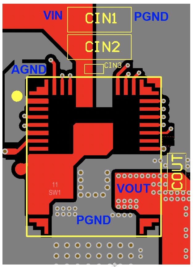
Figure 5: Recommended PCB Layout – Top Layer
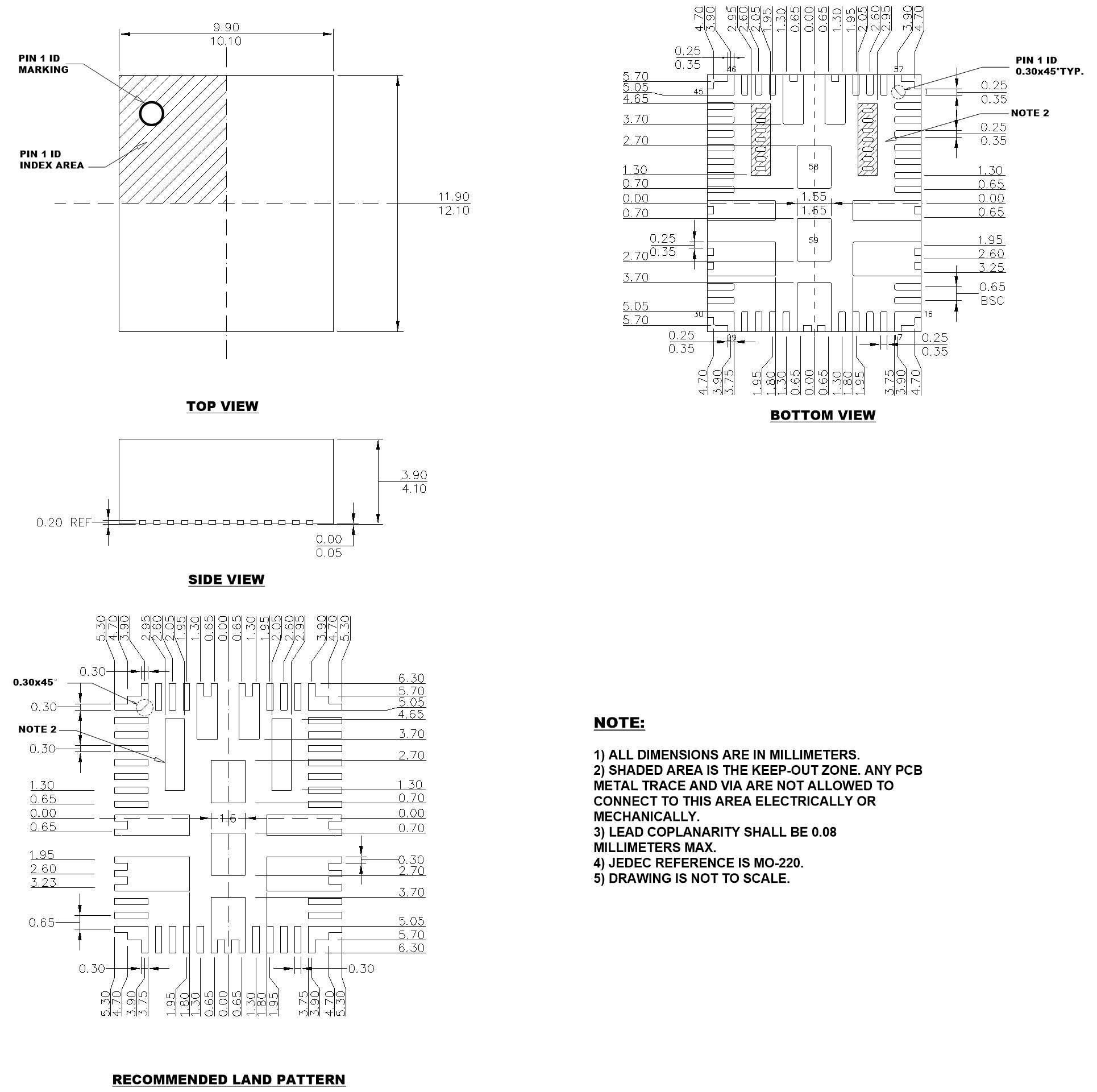
PACKAGE INFORMATION
LGA (15mmx15mmx6mm)
NOTICE: The information in this document is subject to change without notice. Please contact MPS for current specifications. Users should warrant and guarantee that third-party Intellectual Property rights are not infringed upon when integrating MPS products into any application. MPS will not assume any legal responsibility for any said applications.
mEZDPD1620 系列产品为可扩展、可编程 DC/DC 电源芯片,峰值输出电流高达 25A。两种封装尺寸可选:mEZDPD1620A 采用表面贴装(LGA 封装),而 mEZDPD1620AS 采用 DIP封装(双列直插式封装)。
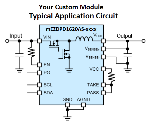
mEZDPD4506AS 具有数字可编程功能,可通过I2C通信总线控制和编程。可编程的工作参数包括:补偿值、输出电压转换速率、开关频率和省电模式。预先配置的DIP封装模块可以提供快速评估。
希望您的自定义配置预加载至评估板吗?先创建并保存一个模块配置,然后订购评估板 点击这里
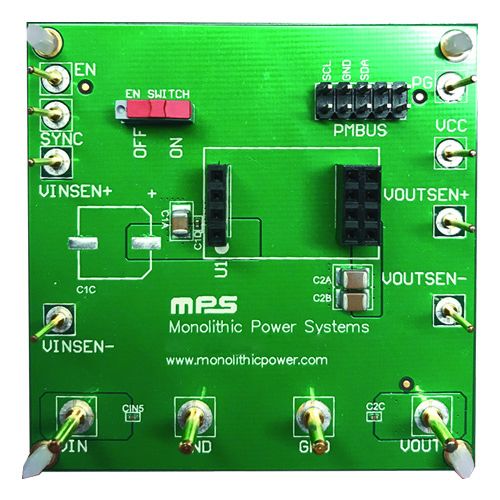
mEZDPD1620A 可配置电源模块评估板
EVmEZDPD1620A 是 mEZDPD1620A 的评估板。mEZDPD1620A 是一款可配置的 DC/DC 电源模块,输出电流最高可达 20A,输出电压范围为 0.6-5.5V。该模块具有可多次编程的存储器,可使用 Virtual Bench Pro GUI进行编程(如下提供)。
使用 GUI 配置并监控产品性能,如输入电压(Vin)、输出电压(Vout)、输出电流(Iout)和温度。评估开始时只需要提供电流和输出电压值。其他参数可使用默认值,也可以根据需要重新配置。
想要将自定义配置预加载到评估模块?点击此处创建和保存模块配置。
¥181.25 + 税
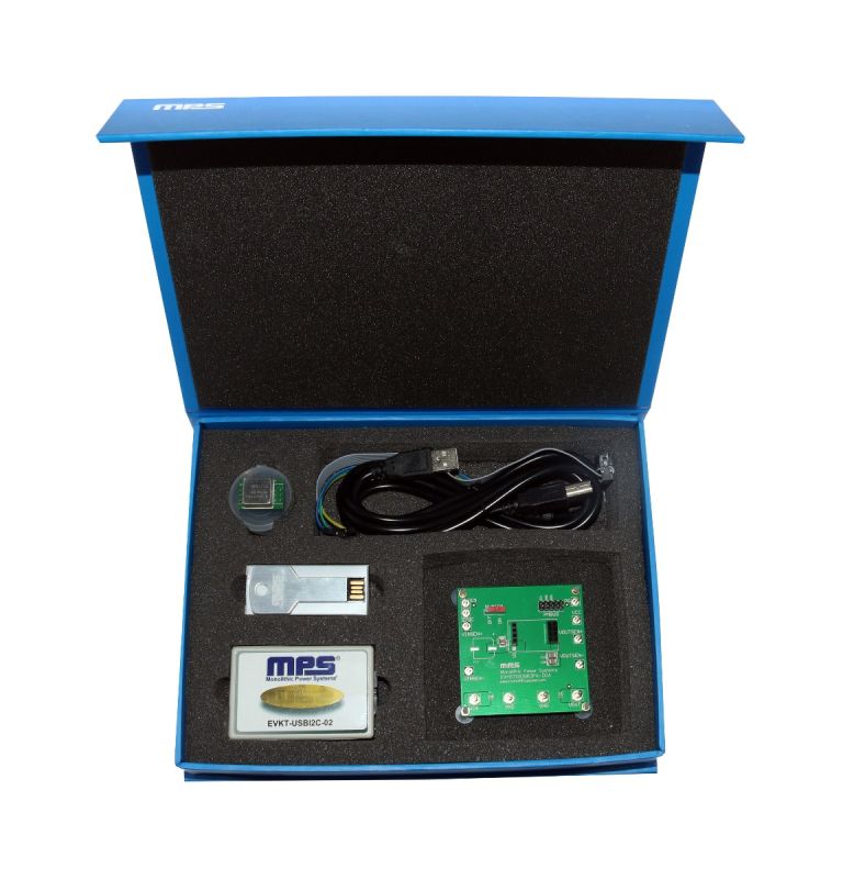
mEZDPD1620A 可配置电源模块评估套件。
PKT-mEZDPD1620A 是 mEZDPD1620A 的评估套件。mEZDPD1620A 是一款可配置的 DC/DC 降压电源模块,输出电流最高可达 20A,输出电压范围为 0.6-5.5V。
该模块具有可多次编程的存储器,可使用 Virtual Bench Pro GUI(图形界面)进行编程(如下提供)。使用 GUI 配置并监控产品性能,如 Vin、Vout、Iout 和温度。评估开始时只需要提供电流和输出电压值。其他参数可使用默认值,也可以根据需要重新配置。
想要将自定义配置预加载到评估模块上?请在此处创建并保存模块配置
¥688.75 + 税
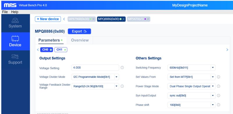
由 MPS 支持的图形用户界面(GUI),用于通过 I2C 接口配置和监控多个 MPS 数字电源解决方案
Virtual Bench Pro 4.0 是一款由 MPS 支持的图形用户界面(GUI),用于通过 I2C 接口配置和监控多个 MPS 数字电源解决方案。此 GUI 是一款直观型工具,可与 MPS 评估套件配合使用,有助于设计评估和测试。
硬件和软件要求:
- USB 转 I2C 通信设备 EVKT-USBI2C-02
- 运行 Windows 10 或更高版本的 PC
- .Net Framework 4.0 或更高版本
- 内存:2GB 可用内存
- CPU:任何现代 CPU
- 磁盘空间:2GB
- 显示器分辨率:1024x768
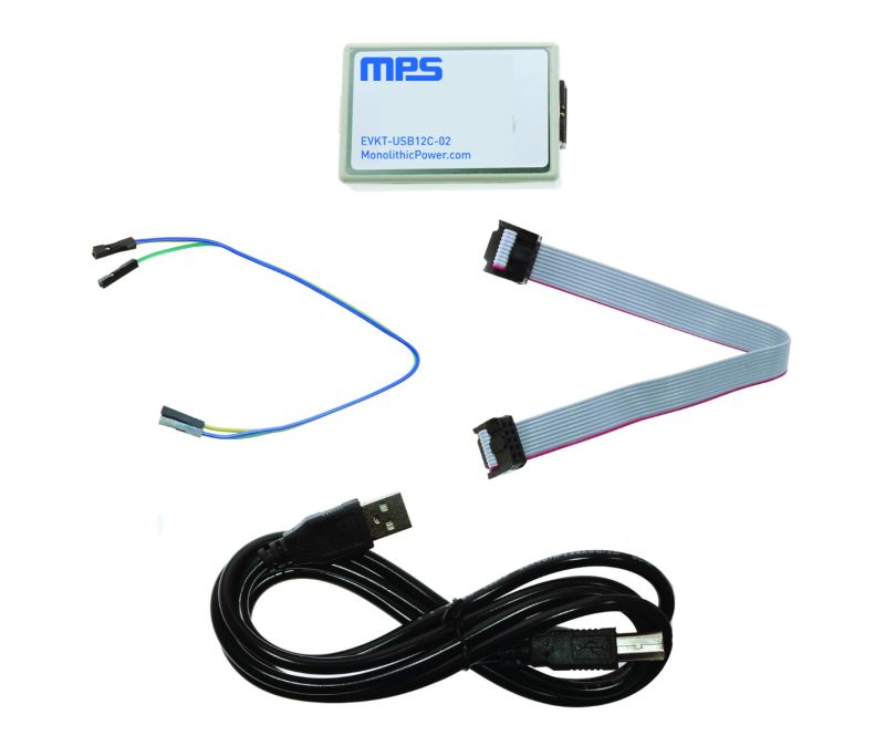
USB 转 I2C/PMBus 通信接口设备,包含在产品评估套件中,也可单独购买
EVKT-USBI2C-02 包含在产品评估套件中,也可单独购买。该通信接口同时兼容USB 转 I2C 端口和 USB 转 PMBus 端口。它是设计用于 MPS I2C 和 PMBus 产品和虚拟平台及 I2C GUI 工具上。与 MPS 虚拟平台和 I2C GUI一起使用可以简单快速地评估 MPS 的数字产品性能。
EVKT-USBI2C-02 套件包括:
- 1 个 USB 转 I2C 通信设备接口
- 1 根 USB 线
- 1 根 10 芯排线
- 1 根 3 芯排线
- 带有规格书和驱动文件的拇指驱动
¥362.50 + 税
技术论坛
 Latest activity 2 years ago
 2 回复
2 回复
 Latest activity 2 years ago
 2 回复
2 回复
 Latest activity 2 years ago
 6 回复
6 回复

 了解更多我们的评估板套件


