AN201 - MP279x ADC 校准指南

每月为您发送最具参考价值的行业文章
我们会保障您的隐私
摘要
MP279x电池监控器系列(包括MP2787 、 MP2790 、 MP2791 、 MP2796和MP2797)支持对单电池电压和电池组电流进行ADC (模数转换器)采样。
电池电压和电池组电流一般通过工厂校准,其校准精度可以在各器件相应的数据手册中获取,但通过系统级校准可以实现更高的精度。本文将对ADC校准进行介绍,包括参数说明和校准指南。
简介
MP279x电池监控器系列(包括MP2787 、 MP2790 、 MP2791 、 MP2796和MP2797 )支持对单电池电压和电池组电流进行ADC采样。其电池电压校准通过比较实际电池电压与测量电压,确定系统微控制器 (MCU) 可以使用的校正系数,从而提高测量精度。该校准基于单电池电压增益的校准过程。
电池组电流ADC校准则通过测量SRP和SRN引脚间电流采样电阻(分流器)两端的电压,从而确定电池组电流。该校准需首先确定偏移量,再计算ADC电流增益。
校准
电池电压校准过程
电池电压校准依赖于电池电压的测量增益。可遵循以下步骤进行电池电压校准:
- 在器件C0和C1引脚之间施加已知电池电压(VCELL, 约为 4000mV)。
- 通过MCU在寄存器0x99 [0]中写入 1 ,以启动高分辨率扫描;
- 读取寄存器0x99 [1];如果0x99 bit[0]= 0x1 ,则 ADC 扫描完成;
- 读取寄存器0x6C [14:0],得到十进制读数(由十六进制转换而来);
- 通过公式(1)计算电池电压增益: $$ \text{增益} = \frac{V_{\text{CELL}}}{\text{读数}} $$
再通过公式 (2) 估算由ADC 计算得到的电池电压 (VCELL_ADC):
$$ V_{\text{CELL_ADC}} = \text{增益} \times \text{读数} $$上述电池电压校准过程仅适用于室温条件 0°C ≤ TA ≤ 25°C)。对于其他温度范围,请使用公式 (2) 对 VCELL_ADC 进行温度补偿校准,以进一步提高精度并最终获得特定温度 (VCELL_TEMPC)下的校准值。其他温度下的校准过程如下所述:
- 如果 TA < 0°C,则使用公式 (3) 的温度补偿计算 VCELL_TEMPC : $$ V_{\text{CELL_TEMPC}} = V_{\text{CELL_ADC}} \times \left( 1 + \frac{T}{40000} \right) $$
- 如果 0°C ≤ TA ≤ 25°C, 则用公式 (4) 估算 VCELL_TEMPC: $$ V_{\text{CELL_TEMPC}} = V_{\text{CELL_ADC}} $$
- 如果 TA > 25°C,用公式 (5) 计算 VCELL_TEMPC: $$ V_{\text{CELL_TEMPC}} = V_{\text{CELL_ADC}} \times \left( 1 + \frac{T - 25}{66666} \right) $$
注:
- LSB替换为校准增益,通过读数乘以增益即可直接得到校准结果。
- 可取多个读数并计算平均值以提高校准精度。
电池电压校准示例
在C0和C1之间施加4000mV (VCELL) ),可得到26233的测量结果。然后通过公式(6)估算增益:
$$ \text{增益} = \frac{V_{\text{CELL}}}{\text{读数}} = \frac{4000}{26233} = 0.152482 $$VCELL_ADC 可采用公式 (7) 来计算:
$$ V_{\text{CELL_ADC}} = 0.152482 \times \text{读数} $$如果温度超出室温范围 (TA < 0°C 或 TA > 25°C)),则更新公式 (3) 和公式 (5)。例如,分别采用公式 (8) 和公式 (9) 来估算-20°C和 +40°C时的 VCELL_TEMPC:
$$ V_{\text{CELL_TEMPC}} = \left( 0.152482 \times \text{读数} \right) \times \left( 1 - \frac{20}{40000} \right) \quad (T = -20^\circ\text{C}) $$$$ V_{\text{CELL_TEMPC}} = \left( 0.152482 \times \text{读数} \right) \times \left( 1 + \frac{40 - 25}{66666} \right) \quad (T = 40^\circ\text{C}) $$
MCU 使用此校准参数(增益)来调整每节电池的读数。
图 1 展示了校准前后室温下不同电池输入电压下的电池测量误差。
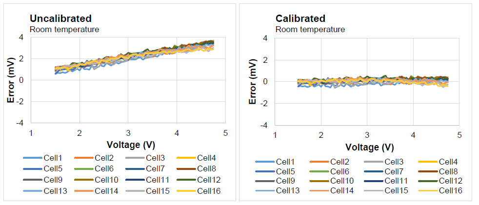
图1:测量范围内的绝对电池电压误差比较(室温)
图2展示了校准前后,当 VCELL = 4V,每个电池在不同温度下的测量误差。校准过程对室温范围以外的数据进行了温度补偿。
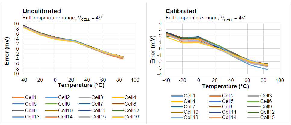
图2: 不同温度下的绝对电池电压误差( VCELL = 4.5V )比较
电池组电流校准过程
遵循以下步骤进行电流校准操作:
- 首先确保SRP和 SRN 引脚间的电流采样电阻上没有电流经过;
- 在0x99 [0]中写入 1 ,以启动高分辨率扫描;
- 如果0x99 [1] = 0x1 ,则 ADC 扫描完成;
- 读取寄存器0x6B [15:0],获得十进制读数1(由十六进制格式转换而来);
- 施加已知电流 (IC, about 1A) 并确保电流流过电流采样电阻 (RSENSE).
- 在0x99 [0]中写入 0,并重复步骤 2 和 3 以获取十进制读数(由十六进制格式转换而来);
- 用公式(10)计算偏移量: $$ \text{偏移量} = \text{读数1} $$
- 用公式(11)估算电流增益:: $$ \text{电流增益} = \frac{I_c}{\text{读数} - \text{偏移量}} $$
分别用公式(12)和公式(13)进行电流 (IADC) 和电压 (VADC) c校准:
$$ I_{\text{ADC}} = \text{电流增益} \times (\text{读数} - \text{偏移量}) $$$$ V_{\text{ADC}} = \text{电流增益} \times R_{\text{SENSE}} \times (\text{读数} - \text{偏移量}) $$
注:
电池组电流校准示例
本例中,RSENSE 取值 200mΩ。当SRP和 SRN 之间没有电流流过时,电池组电流 ADC 测量值即为偏移量,如公式 (14) 所示:
$$ \text{偏移量} = \text{读数1} = -9\ (\text{DEC}) $$在 RSENSE上施加500mA电流(流经SRP和 SRN 之间) ,并利用公式 (15) 估算下一个读数:
$$ \text{读数} = -31669, \quad V_{\text{SRN} - \text{SRP}} = -96.18\,\text{mV} $$用公式(16)计算电流增益:
$$ \text{电流增益} = \frac{V_{\text{SRN} - \text{SRP}}}{\text{读数} - \text{偏移量}} = \frac{-96.18}{-31660} = 0.003038 $$用公式(17)估算 VADC:
$$ V_{\text{ADC}} = 0.003038 \times (\text{读数} - \text{偏移量}) $$图3展示了校准前后室温下不同 VSRP_SRN 下的电流测量绝对误差比较:
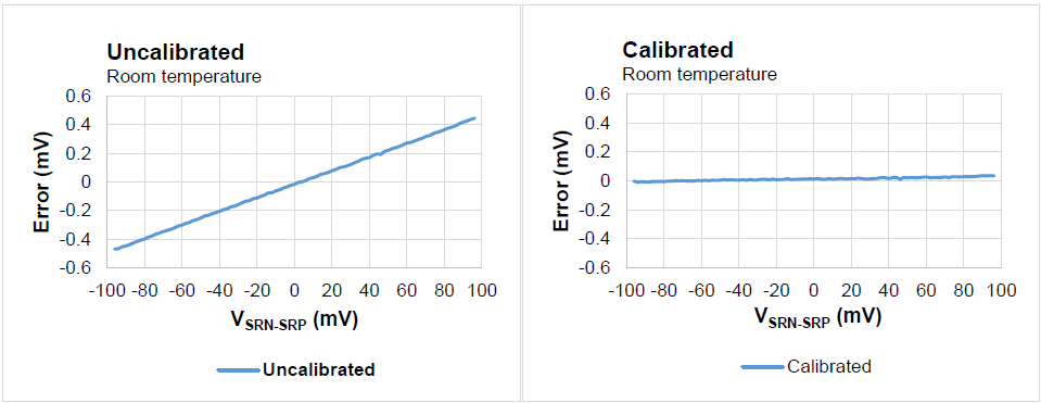
图3:测量范围内的绝对电池组电流误差比较
图4展示了校准前后室温下不同 VSRP_SRN 下的电流测量相对误差比较。
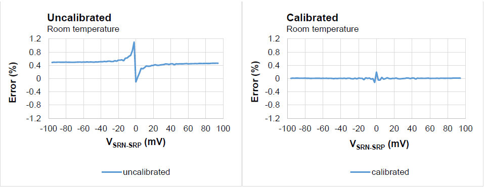
图4:测量范围内的相对电池组电流误差比较
校准前后,不同温度下、不同 VSRP_SRN 下的电流测量绝对误差比较如图5所示。
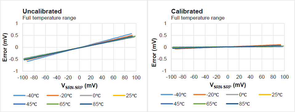
图 5:全温范围内的绝对电池组电流误差比较
校准前后,在 VSRP_SRN = ±90mV, ±60mV, ±30mV时、不同温度下的电流测量相对误差比较如下图所示。
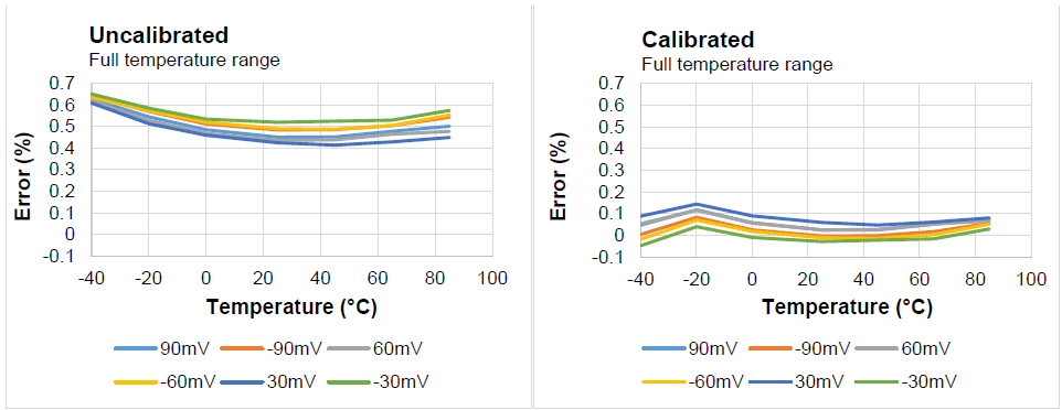
图6:全温范围内的固定电流点相对测量误差比较
总结
表1展示了电池电压测量误差比较。
表1:电池电压ADC误差比较
| T (°C) | 室温 | -40°C 至 +85°C | -20°C 至 +65°C |
|---|---|---|---|
| 数据手册规格(电池电压误差,未校准) | ±5mV | ±12.5mV | ±7.5mV |
| 示例单元(电池电压误差,未校准) | ±4mV | ±10mV | ±6mV |
| 示例单元(电池电压误差,已校准) | ±1mV | ±5mV | ±3mV |
VCELL = 4.5V时,65 个芯片校准前后在不同温度下的电池测量误差比较如图7所示。
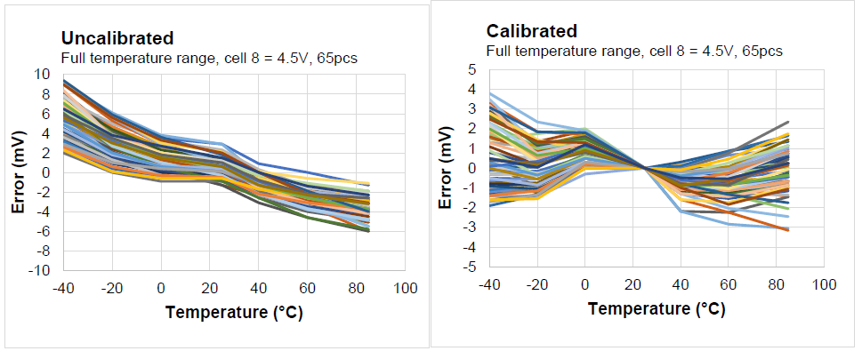
图7:全温范围内65 个芯片的电池8(4.5V )绝对测量误差比较
表2展示了电池组电流测量误差对比数据。
表2:电流ADC误差比较
| 温度 (°C) | 室温 | -40°C 至 +85°C |
|---|---|---|
| 数据手册规格(电池组电流误差,未校准) | ±0.5% x 读数 ±35μV | ±1% x 读数 ±35μV |
| 示例单元(电池组电流误差,未校准) | ±0.2% x 读数 ±35μV | ±0.7% x 读数 ±35μV |
| 示例单元(电池组电流误差,已校准) | ±0.1% x 读数 ±6μV | ±0.2% x 读数 ±6μV |
图 8 显示了校准前后 65 个芯片在不同温度下的电池组电流测量误差。
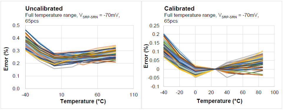
图8:65 个芯片在全温范围内的相对电池组电流误差(VSRP-SRN = -70mV)比较
由此可见,根据本文提供的方法进行校准后,电池电压和电池组电流测量结果可以得到显著改善。
结语
本文介绍了MP279x系列电池监控器的电池电压和电池组电流测量校准方法和步骤。电池电压校准之后,室温 (TA)下的误差可降至 ± 1mV以内;全温范围内的校准前误差为 ± 12.5mV ,校准后误差则在 ±5 mV 以内。对电池组电流测量进行校准之后,室温下的电池组电流测量误差可降至 ±0.1% x (读数 ± 6μV ),全温范围内误差可降至 ±0.2% x (读数 ± 6μV )。
_______________________
您感兴趣吗? 点击订阅,我们将每月为您发送最具价值的资讯!
技术论坛
 Latest activity 11 months ago
 8 回复
Latest activity 2 years ago
1 评论
Latest activity 2 years ago
1 评论
8 回复
Latest activity 2 years ago
1 评论
Latest activity 2 years ago
1 评论
直接登录
创建新帐号