AN169 - MP2696A Power Bank Reference Design

Get valuable resources straight to your inbox - sent out once per month
We value your privacy
Abstract
Power banks have been popularly used as an auxiliary device for years due to the conflict between the increasing of the portable device performance and the limit of the battery size and capacity. A fine power bank design appreciates compact shape, high reliability, high power conversion efficiency and rich phone compatibility, etc. This application note introduces a highly integrated power bank design based on MP2696A, and also provides design guides for a quick, turnkey solution.
Introduction
Overview
The MP2696A is a flexible battery charging and reverse discharging IC for single cell battery applications. It is specially designed for a high performance power bank with all the necessary functions, the external components are minimized and integrated. MP2696A offers rich software programmability, with a most economical and simplest microcontroller (MCU), a compact and fully functional power bank can be easily designed and delivered in a short time.
Depicted in figure 1, the MP2696A integrates 4 power MOSFETs: reverse blocking MOSFET (Q1), output blocking MOSFET (Q2), high side switching MOSFET (Q3) and low side switching MOSFET (Q4). Utilizing MPS proprietary fabrication and packaging process, the device offers superior conversion efficiency in a 3mm*3mm compact package. In advance, those MOSFETs’ voltage ratingare all up to 16V, which offers superior reliability in 5V USB applications. The MP2696A utilizes single inductor to work either in buck or boost converter mode to control the battery charging and discharging, while managing input and output port power deliveries with rich protection functions.
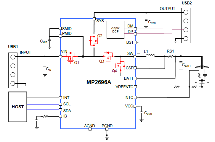
Figure 1: MP2696A Simplified Application Circuit
Operation Mode Description
The operation mode of the device can be categorized into 4 conditions:
1, idle mode, during which the device is in power saving mode, all 4 MOSFETs are off, the VCC regulator is alive and the I2C communication is ready to take commands from the host. In this condition, the device minimizes the battery current consumption at typically 25µA, which minimizes the battery discharge current during storage or shelf time.
2, charge mode, during which the device charges the battery utilizing the power from input source (typically a USB port), the MOSFET Q1 is turned on, and the switching MOSFET Q3 and Q4 works as a buck converter to charging the battery. Depending on the battery voltage, the charging phase can be in pre-charge, constant current charge or constant voltage charge status. The charging current and battery regulation voltage can be programmed in the registers. When the battery is fully charged, the device enters charge termination mode, in which the buck regulator stops and MOSFET Q1 keeps on.
In charge mode, there are 4 loops regulating the buck converter: charge current, charge voltage, input current and input voltage. Any of them can limit the output power from the buck converter to the battery so that the max power delivered will not exceed the design values.
3, boost mode, during which the device generates a 5V (typical) output utilizing the battery power, the MOSFET Q1 is off, the switching MOSFET Q3 and Q4 works as a boost converter to deliver a regulated voltage on PMID pin, then the output blocking MOSFET (Q2) passes the PMID power to SYS pin. SYS pin is the power output port of the device and so as the power bank.
In boost mode, there are 2 loops regulating the boost converter: output voltage at PMID node, output current in MOSFET Q2. Any of them can limit the boost converter output power, so that the power bank output will behave as a constant voltage / constant current (CV/CC) output port. Both the output voltage and the max output current can be programmed in registers.
4, pass through mode. When input source is present and is charging the battery, if the host also turns MOSFET Q2 on, the device can also deliver output power at SYS port. The SYS power is delivered from input source through Q1 and Q2 (in series). This application case is for that the end user can charge the power bank and the phone together.
In pass through mode, the battery charging current and the SYS port load current share the input source power. Since the SYS port load current is dependent on that the phone draws, SYS output is prioritized, which means, given that the input current loop and input voltage loop of the device limits the max power that the input source can provide, the battery charge current would taper if any of above 2 loops is touched. Please be noted that the MOSFET Q1 or MOSFET Q2 does not provide regulation function, so if the SYS port load exceeds the input current limit, battery charge current will reduce to zero while Q1 and Q2 will stay on.
Protections
1, input over voltage protection: the device support 2 levels of input over voltage protection. The default value is 6V and can be programmed to 11V in REG07h bit[3]. Once input voltage is higher than the protection threshold, the part stops switching. For normal USB based input operations, the 6V OVP threshold provides superior reliability. And when the input OVP is set to 11V, the device can charge with a higher voltage input source such as a 9V adaptor, which can provide higher charging current. Please note that even if input OVP is set to 11V, the MOSFET Q2 will be automatically disabled when input is above 6V. This prevents the device delivering high voltage to SYS port which might be dangerous for SYS port load.
2, SYS port short circuit protection: during boost discharging or pass through mode, the SYS port is delivering power output. In case that there is a hard short circuit on SYS node, to prevent the device from damaging, a fast short circuit protection is always alive as long as MOSFET Q2 is on. The fast short circuit protection threshold is set to relatively high as 8A. In any time the current in MOSFET Q2 touches this threshold, the MOSFET Q2 is turned off immediately. And after a 300ms hiccup time, the MOSFET Q2 tries to start up again.
Feature and Design
MPPT for Maximizing Charge Speed
The input source of power banks are usually from a USB port. There are multiple kinds of USB ports offering different levels of maximum output current, defined by Battery Charging Specification Revision 1.2 (BC1.2), or USB Type-C Specification or some vendor’s proprietary specification. Those USB ports starting voltage are always 5V (typical value) and offers an output current limit depending their capability. In MP2696A reference design, to maximize the battery charging speed, Maximum Power Point Tracking (MPPT) is chosen as a convenient method.
The MPPT approach is shown below with MCU’s control:
1. Host presets the ICC current setting to 500mA, IIN_LIM to 3000mA, VIN_MIN to 4.65V.
2. If an input source is plugged in, USB1_PLUG_IN (REG05h bit[1]) will be set to 1 with an interrupt (INT) pulse, charging automatically starts.
3. If CHG_STAT=10, (REG05h bit[5:4]), host tries ramping up ICC, 100mA per 1 second.
4. If the input source drops to VIN_MIN threshold, VPPM_STAT (REG05h bit[3]) will be set to 1 with an INT pulse. Host can also keep reading REG05h to monitor the status.
5. Host reduces the ICC by 100mA per 125ms till VPPM_STAT (REG05h bit[3]) returns to 0, then the device keeps charging the battery with that ICC value.
6. Host repeats the #3-#5 every 10 seconds.
7. If anytime the input source is un-plugged (USB1_PLUG_IN=0, REG05h bit[1]), or the charging is terminated (CHG_STAT=11, REG05h bit[5:4]), host resets the ICC setting to 500mA.
With the above approach, the power bank keeps drawing the maximum power that the input source can provide. The max input current will not exceed 3A that set in IIN_LIM register, which makes the USB receptacle, plug and cable safe, and it offers good compatibility among various kinds of USB ports without complex protocol design.
Battery Thermal Management
Among the rechargeable batteries, Li-ion batteries provide high volumetric and gravimetric energy densities, also they have a low self-discharge rate and high instant discharge capability. But as a chemical based components, temperature is a crucial thing for the battery’s safe operation especially during the charging progress. Fire or explosions of Li-ion batteries’ thermal run-away result that being reported should definitely beavoid in the power bank designs. To well manage the thermal related safety concern, progress has been made in industry standard such as the Japan Electronics and Information Technology Industries Association (JEITA) guide lines.
If the battery’s surface temperature becomes lower than COOL threshold (10°C as an example), high charge current can cause permanent loss of the lithium ions and degrades the battery faster. Therefore, the recommended approach is to reduce the charge current during this temperature region. If the temperature is further reduced to below COLD threshold (0°C as an example), the charging should not be allowed, as shown in figure 2.
If the battery’s surface temperature becomes higher than WARM threshold (45°C as an example), the cathode material gets more active and can chemically react with the electrolyte when the cell voltage is high, it also degrades the battery. The recommended approach is to reduce the charge voltage during this temperature region. If the temperature is further rising up to above the HOT threshold (60°C as an example), the charging should not be allowed to prevent battery thermal run-away, as shown in figure 3.
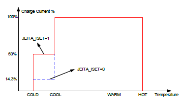
Figure 2: JEITA Profile – Charge Current
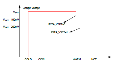
Figure 3: JEITA Profile – Charge Voltage
The MP2696A offers fully customized JEITA profile. The battery temperature can be sensed by a thermistor driven by VRNTC output. When the device is switching, the VRNTC outputs a voltage which biases the thermistor with a resistor divider. The NTC pin’s voltage is compared with internal thresholds for detecting the battery temperature. The device can automatically stop charging if the temperature is out of the HOT or COLD threshold, or reduce the charge current or charge voltage according to the register settings in COOL or WARM range. The NTC function can be enabled or disabled in EN_NTC,REG01h bit[2], the JEITA function can be enabled or disabled in JEITA_DIS, REG02h bit[3], the JEITA temperature thresholds and charge current/voltage reducing magnitudes can be adjusted in REG08h.
Output Port ON/OFF Control
The SYS output is for the output USB port to deliver power to external load such as mobile phones. The output USB port should start to deliver 5V when a phone is connected, but to minimize the battery’s discharge when the power bank is in idle mode, the boost converter and the output USB port should be in off status when there is nothing plugged in. The MP2696A provides an integrated load detection function to manage those functions with host’s intervention.
During idle mode, if the register bit USB2_EN_PLUG, REG04h bit[1], is enabled, a resistor (typical value 1.5kΩ) is connected between BATT pin and SYS pin. This resistor charges up the SYS pin capacitor to be same as the battery voltage, since there is no load on SYS node, this SYS float voltage does not have battery current consumption. After the SYS pin voltage is charged up to 90% of the battery voltage, a comparator of 75% of battery voltage is enabled. In this condition the MP2696A is ready to detect the SYS load plug in event.
When a load such as a phone connects into the SYS USB port, the SYS node floating voltage will be pulled down due to the load current consumption or load input capacitance. This will trigger the 75% comparator, MP2696A can detect this and set USB2_PLUG_IN, REG04h bit[0], to 1, with an interrupt pulse followed on INT pin. Hostresponding the interrupt by reading REG04h can know this event and can turn on the boost and MOSFET Q2 to enable the SYS power output.
Once set, the USB2_PLUG_IN bit will keep at 1 regardless of the 75% comparator status, host need to write 1 to this bit to clear it to 0.
After the host enabling the boost and MOSFET Q2, host should also write USB2_EN_PLUG bit to 0 to disable the detection and the BATT-SYS resistor, in this condition the MP2696A keeps delivering SYS output.
The SYS port output will keep alive as long as battery is not depleted, but if the load is un-plugged or not consuming power, the power bank need to go back to idle mode to save the battery current consumption. The MP2696A integrates a no-load-detection comparator to achieve this.
The current flowing out in MOSFET Q2 is kept monitored when Q2 is enabled, the current in Q2 is compared with a threshold programmed in NOLOAD_THR bits, REG07h bit[7:6], ranging from 30mA to 100mA. If the current in Q2 is less than the comparator value, the NO_LOAD bit, REG03h bit[0] is set to 1 with an interrupt pulse followed on INT pin. The host can acknowledge this by reading the REG03h, and host can enable a timer if the no load condition exist. If the no load condition last for a duration such as 20 seconds, the host can turn off the boost and MOSFET Q2 to enter idle and power saving mode.
After the idle mode is entered, host can re-enable USB2_EN_PLUG bit to enable next plug-in event detection.
During charge mode, the SYS load plug in detection can also be effective. The host can also get the SYS plug in event information and turn on boost and MOSFET Q2. Note that if boost is enabled (BST_EN=1) when input is present, the MP2696A will keep working in charge mode, boost is ignored. In this case the device works in pass through mode, battery is being charged and SYS port voltage is supplied by the input source.
Only when input source voltage is unplugged and IN pin voltage drops below 2V, the boost can then start automatically if BST_EN=1.
Please also note that there will be a tens of milliseconds drop on SYS output when input is un-plugged, MP2696A does not support seamless transition between charge mode and boost mode.
Output Signaling
As a USB output port, the SYS output delivers power to external load such as mobile phones. The phones usually have protocols to distinguish the USB ports’ type and output capabilities to determine its power consumption limit. For example, the phone can distinguish the port between computer USB port (SDP) or a Dedicated Charger Port (DCP) to set its input current limit. The MP2696A integrates output signaling on DP/DM pins to imitate a proper USB port, which can maximize the load charging speed.
Once SYS output is enabled by host, the DP/DM pins are tied to an internal 2.7V output buffer via a 30kΩ resistance, respectively. This imitates an APPLE 2.4A adaptor, if an APPLE device is plugged in, that device can charge with its maximum speed.
If an ANDROID device is plugged in, that device will start BC1.2 progress to distinguish the type of USB port. MP2696A’s DP/DM pin can detect the load device’s BC1.2 request and switch to a Dedicated Charging Port (DCP), in which the DP/DM pins are tied together with a 100Ω resistor. Hence the ANDROID device can also charge with its maximum speed.
The DP and DM pins are designed to be enhanced with an 8000V human body mode ESD level, which provide superior reliability when connected on physical port receptacle.
Max Discharge Power
When the device is working in boost discharge mode, the SYS port output acts as a constant voltage / constant current (CV/CC) output. The SYS port delivers a regulated output voltage (5V adjustable) and a max output current limit (2.1A to 3.6A adjustable). If the SYS port load reaches the output current limit, the SYS output voltage will decrease and keep the output current within the preset limit (CC operation). However, as the SYS port’s power is generated by boosting from the battery, the CC operation range should be above the battery voltage. If the output voltage drops below the battery voltage, the boost output will stop and hiccup. However, this 5V to battery voltage region is typically enough for an effective output constant current (CC) operation.
The max output current is not only limited by the register setting (IOLIM), but also limited by the max switching MOSFET current. There is a peak current limit at the low side switching MOSFET Q4, (programmable from 5A to 6.5A). The current in MOSFET Q4 is limited cycle by cycle with this hard limit. In case the battery voltage is low, the max discharge power is limited by this peak current, it can be roughly calculated as:
$$ I_{\text{discharge_MAX}} = I_{\text{peak_MAX}} - \frac{\Delta I_{\text{inductor}}}{2} $$Where the Ipeak_MAX is the peak current limit of MOSFET Q4, ΔIinductor is the peak to peak inductor current ripple, Idischarge_MAX is the max battery discharge current. By configuring the BST_IPK bits, REG07h bit[1:0], the maximum battery discharge current can be programmed.
The benefit of this setup is, when battery voltage is low, the maximum discharge power can be limited, which also limits the battery thermal rise and also the power bank thermal performance (user experience), it also reduces the battery degrading speed. Please note that during this condition, the maximum output current might not be able to reach to the value programmed in the IOLIM bits.
SYS Port Cable Drop Compensation
The SYS port is typically a USB output port for powering external device via a USB cable. The MP2696A is regulating the PMID voltage for the SYS port output voltage, however, since the USB cable has resistive voltage drop, the voltage on load device’s USB receptacle would drop as the current flowing in the cable increases, which might limit the load device’s charging speed. The MP2696A offers a convenient method to improve this performance by integrating a cable compensation option. Programmed in RSYS_CMP bits, REG03h bit [3:1], the current flowing in MOSFET Q2 is sensed, and the PMID regulation voltage is linearly increased according to the SYS port output current. The equation is:
$$ V_{\text{PMID}} = V_{\text{BOOST}} + \left( I_{\text{SYS}} \times R_{\text{SYS_CMP}} \right) $$where VBOOST is the no load output voltage set by REG04h bit[7:5], ISYS is the current in MOSFET Q2, RSYS_CMP is the compensation magnitude set by REG03h bit[3:1], and VPMID is the PMID pin regulation voltage. The RSYS_CMP value can be configured according to each design to achieve a good SYS cable compensation function.
Components Selection
The MP2696A is not very sensitive to external components values, general guidelines are list as below:
1, a 1µH inductor is OK for most of applications. The inductor’s saturation or thermal limiting current should be higher than the inductor peak current (6.5A for example).
2, given all the input port capacitance limitation, place a 1µF capacitor at IN pin, and the rest capacitance on PMID pin.
3, the SYS port output capacitor have much more freedom, but too much capacitance may affect the SYS load plug in detection function, it is suggested to be tested case by case.
4, the current sensing resistor is recommend asa 10mΩ resistor in 0805 package, please be noted the current sensing signal need to be routed with kelvin sensing traces.
PCB layout and EMI concerns
PCB layout is essential for not only the proper operation, but also has great relationship with the power bank’s EMI performance. Please follow below guidelines to get the best result:
1, PMID capacitor routing. The key point is to minimize the “hot loop” of the high frequency switching current. As shown in figure 4, the high side switching MOSFET Q3 and low side switching MOSFET Q4 construct a switching bridge. During the switching transient, the current passing in the switching MOSFETs has an ultra-fast current changing speed (di/dt), this fast changing current induces magnetic field into the PCB and space and is the source of the EMI generation. The di/dt is in nano seconds level and it has rich harmonic components. The most important thing is to make this fast changing current limited in as small area as possible on the PCB, which means, minimize the loop shown in figure 4. In another word, connect the PMID capacitor’s positive terminal as short as possible to the PMID pin, and connect the PMID capacitor’s negative terminal as short as possible to the PGND pin. In real application, the best way is to use a 1206 size PMID capacitor to locally bypass the switching bridge, and the SW trace can be routed beneath the PMID capacitor. If the above approach can not be achieved, the second choice is to use vias to connect the PMID capacitor’s ground node to IC’s PGND pin, this requires enough vias, and please also mention thecurrent-flowing route should be as short as possible. Please refer to EV2696A-Q-00A documentation for a reference.
2, minimizing the noisy PGND plane. Even with above local bypassing method of the PMID cap, the PGND plane is still noisy comparing to the PCB quiet ground, it is recommended to minimize the PGND plane and try to isolate it from PCB ground plane, this can also help limit the noise in “cave”.
3, it is not recommended to directly connect AGND to PGND beneath the IC, AGND pin is recommended to be tied to the quite PCB ground plane.
4, for improving EMI performance, extra components can be added such as switching node snubbers and magnetic beads. An 1nF/2.2Ω snubber can be tried as a starting value, please route the snubber to PGND plane and please take care of that the snubber directly increase IC’s thermal rise.
5, magnetic beads are usually helpful for the EMI performance when the SYS port is discharging. The magnetic beads location is recommended as shown in figure 5. Usually bead1 is enough for the first try, and bead2 is also recommended for reserving a PCB space for further improvement, it can be shorted by a 0Ω resistor if not used.
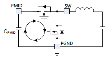
Figure 4: Hot Switching Loop
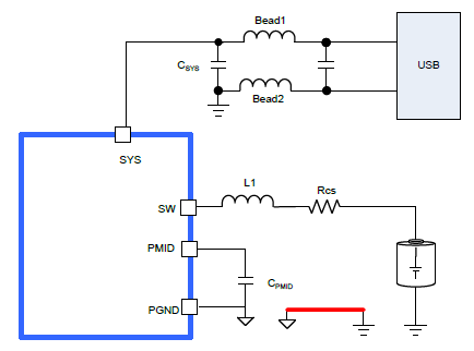
Figure 5: Magnetic Bead Location
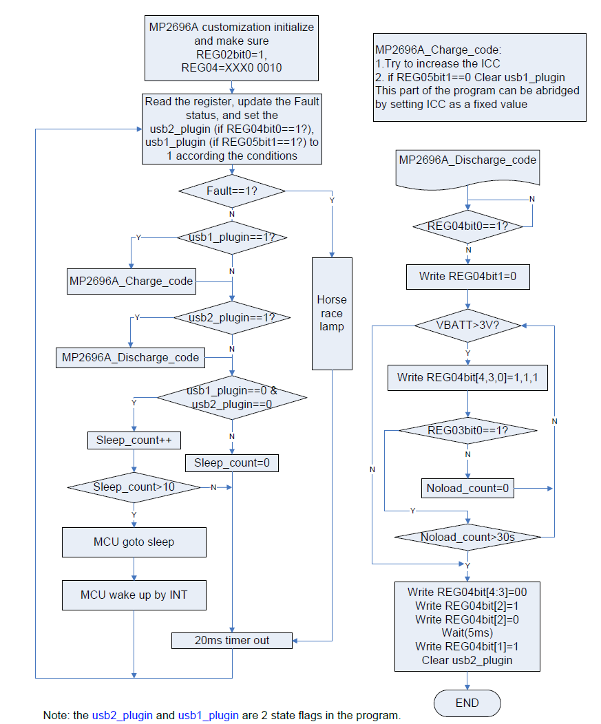
MCU Coding
The MP2696A offers great flexibility for MCU control, a reference code is built in the MCU on EV2696A-Q-00A. Please contact MPS for the EV2696A-Q-00A MCU code.
The simplified coding flow chart is shown below.
MP2696A Code Flow Chart
Conclusion
MP2696A is a turnkey solution for high performance, high reliability and easy-to-use power bank designs. It offers robust power stages for charging and discharging the battery, and also all the necessary analog/digital functions that required to build a power bank.
Additional Reading
For more information about MPS battery management products, please visit this page.
_______________________
Did you find this interesting? Get valuable resources straight to your inbox - sent out once per month!
技术论坛
 Latest activity 5 years ago
 2 回复
Latest activity a year ago
3 回复
Latest activity a month ago
9 回复
2 回复
Latest activity a year ago
3 回复
Latest activity a month ago
9 回复
直接登录
创建新帐号