如何设计超宽输入电压范围反激式变换器

引言
在现代技术中,反激式变换器是家庭和工业应用中广泛使用的拓扑结构之一,常用于需要辅助电源的场景。这种拓扑如此流行,设计者们常常会尝试创建具有超宽输入电压范围(VIN)的统一单设计方案,以最大限度发挥反激式变换器的功能,同时避免长期验证问题。
本文将介绍如何利用MP023来设计具有超宽输入电压范围的反激式变换器。MP023 是一款适用于低功率应用的原边调节(PSR)控制器,它能够提供精确的恒压和恒流输出。我们将以 MP023 为例,展示一个 15W/5V 反激式变换器的设计,该变换器可接受交流和直流输入电压,并支持在宽输入电压范围内工作。
MP023:原边调节反激式控制器
MP023 是一款离线式原边控制器,它能够提供极佳的集成调节功能,无需光耦合器或副边反馈电路。
MP023 的可变关断时间控制使反激式变换器能够在断续导通模式(DCM)下工作。该器件的电流限制和最大副边占空比均可配置,因此输出电流(IOUT)的设置也变得很简单。图 1 展示了 MP023 的典型应用电路。
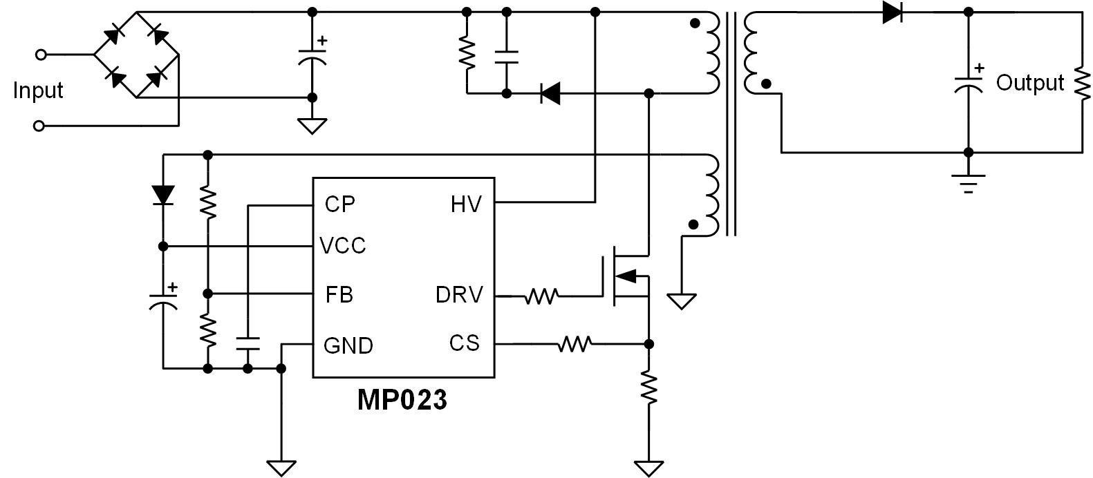
图1: MP023典型应用电路
MP023通过内部高压启动电流源和节能技术将空载功耗限制在 30mW 以下,同时提供全面的保护功能,包括VCC欠压锁定 (UVLO)保护、过载保护 (OLP)、过温保护 (OTP)、开环保护 (OCkP) 和过压保护 (OVP)。
反激式变换器的设计流程
设计具有超宽VIN范围的反激式变换器需要考虑并权衡很多重要因素。下文将详细介绍设计流程中的每个步骤。
图 2 所示为反激式变换器的设计流程图。
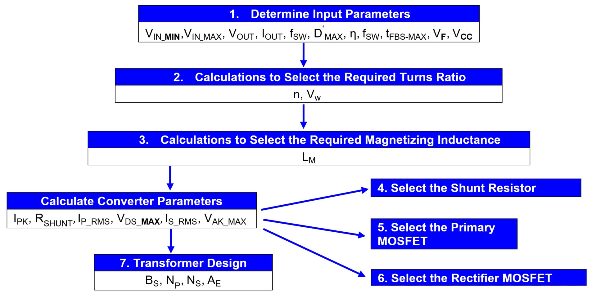
图 2:控制环路设计流程图
反激式变换器的设计流程与相关计算
步骤 1:设计输入
设计变换器需要首先确定输入参数。这些参数包括输入电压(VIN)、输出电压(VOUT)、输出电流(IOUT)、工作模式、开关频率(fSW)、副边占空比、估计效率、反馈 (FB) 最大采样时间、副边 FET 的正向电压以及 IC 电源电压。
表 1罗列出了本文讨论电路的设计输入。在本例中,输入电压范围为85VAC至576VAC,或90VDC至815VDC,可以是交流或者直流输入。
表1:设计输入一览
| 设计输入 | 值 |
| 最小输入电压(VIN_MIN) | 85VAC(或90VDC) |
| 最大输入电压(VIN_MAX) | 576VAC(或815VDC) |
| 输出电压(VOUT) | 5V |
| 输出电流(IOUT) | 3A |
| 操作模式 | DCM |
| 开关频率(fSW) | 50kHz |
| 副边占空比(D’MAX) | 40% |
| 预估效率(η) | 85% |
| 整流管MOSFET正向电压(VF) | 0.1V |
| IC 电源电压 | 12V |
MP023 具有输出电缆补偿功能,根据连接到 CP 引脚的电阻或电容,副边占空比可限定为特定的值。如MP023 数据手册所述,将 1µF 电容连接到 MP023 的 CP 引脚会将副边占空比限制为 40%。
为了确保结果符合实际应用,变换器的预估效率被定义为相对较低(约 85%),这是低功耗反激式变换器的常见效率值。在本应用中,IOUT被定义为 3A,且同步整流控制器(例如 MP6908A)与副边 MOSFET 配合工作以提高效率并改善散热。
步骤 2:计算并选择所需匝数比
由于副边最大占空比有所限制,因此需要根据指定的VIN_MIN计算最大匝数比 (n),以提供足够的IOUT。最大匝数比可以通过公式 (1) 来计算:
$$\begin{align*} n &< \left(1 - D'_{\text{MAX}}\right) \times V_{\text{DC}} / \left(V_{\text{OUT}} + V_F\right) \times D'_{\text{MAX}} \\ &\rightarrow n < \left(1 - 0.4\right) \times 90 / \left(5 + 0.1\right) \times 0.4 \\ &\rightarrow n < 26.47 \end{align*}$$计算出最大匝数比,以VIN_MIN提供最大功率,然后选择合适的 n。最大匝数比的选择需要在副边 RMS 电流和副边 MOSFET 最大反向电压之间进行权衡。
本例利用了同步整流,因此副边 MOSFET 的反向电压很重要,因为低压 MOSFET 具有高性价比且更容易获得。本设计选择的最大匝数比为15;我们将在步骤 5 中对其进行验证。
接下来,计算原边绕组在开关周期的后半部分将经历的输出反射电压(VW)。VW可以通过公式 (2) 来估算:
$$V_w = n \times (V_{\text{OUT}} + V_F) = 15 \times (5 + 0.1) = 76.5V$$VW对计算原边 MOSFET 的最大反向电压很重要。
步骤 3:计算并选择所需磁化电感
由于补偿器的无源元件集成在控制器内部,因此 MP023 可以对其提供的辅助电压进行采样,以实现闭环增益系统(反激式变换器和集成补偿器)。FB 最大采样时间定义了控制器对辅助电压进行采样以进行调节的时间(见图 3)。
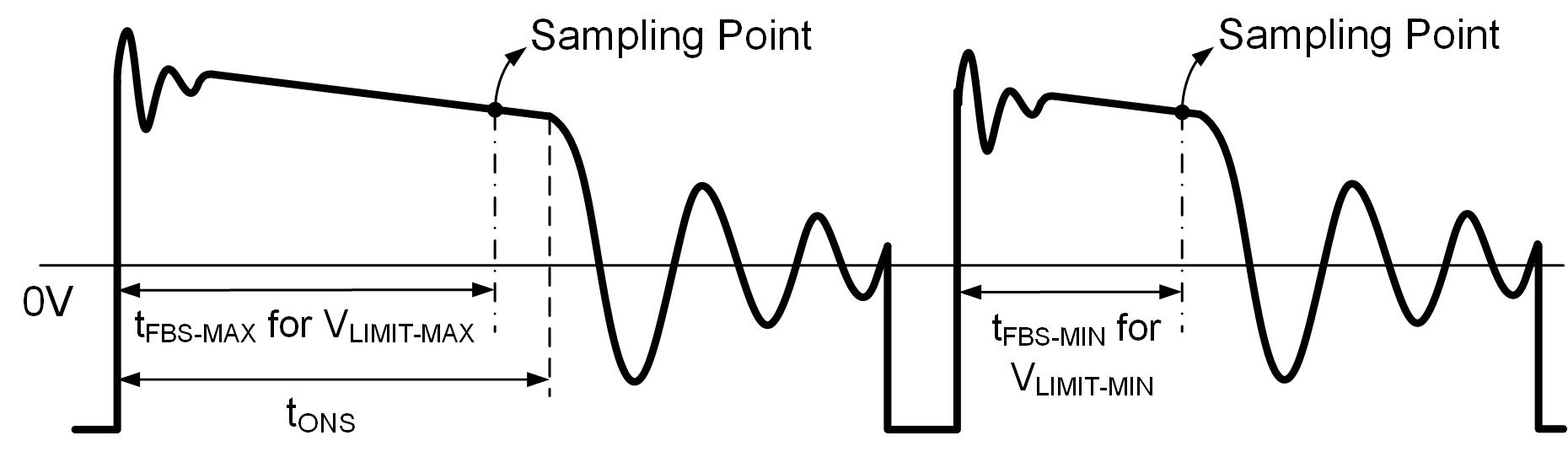
图 3:FB 电压采样点
MP023副边 MOSFET 的最小导通时间(tS_ON)必须满足公式 (3) 中的要求:
$$t_{\text{S_ON}} = I_{\text{PK}} \times \frac{N_{\text{S}} \times L_{\text{M}}}{(V_{\text{OUT}} + V_{\text{F}}) \times N_{\text{P}}} > t_{\text{FBS_MAX}} + t_{\text{FBS_SD}}$$其中tFBS_MAX为 FB 最大采样时间,tFBS_SD为 FB 采样持续时间。
磁化电感及其峰值电流值的计算则需要考虑工作模式。在本例中,MP023 工作在 DCM 模式下,因此可以使用公式 (4) 来估算输出功率 (P):
$$P = \eta \times \frac{1}{2} \times L_{M} \times I_{PK}^2 \times f_{SW}$$根据公式 (3) 和公式 (4) ,最小磁化电感可以通过公式 (5) 来计算:
$$L_{\text{M_MIN}} > \left( \frac {(t_{\text{FBS_MAX}} + t_{\text{FBS_SD}}) \times N_{PS} \times (V_{\text{OUT}} + V_F) \times \sqrt{f_{SW}}} {\sqrt{2 \times P_{OUT}}} \right)^2$$带入值进行计算:
$$L_{\text{M_MIN}} > \left( \frac{(3.5 \times 10^{-6} + 330 \times 10^{-9}) \times 15 \times (5 + 0.1 ) \times \sqrt{50 \times 10^3}} {\sqrt{2 \times 5 \times 3}} \right)^2 \rightarrow L_{M} > 143.1 \mu H$$计算出应用所需的最小磁化电感后,再计算其最大值,该值受固定最大副边占空比的限制。可以公式 (7) 来计算LM_MAX:
$$L_{\text{M_MAX}} < \left( \frac {(D'_{\text{MAX}} \times \frac{1}{f_{SW}}) \times N_{PS} \times (V_{\text{OUT}} + V_F) \times \sqrt{f_{SW}}} {\sqrt{2 \times P_{OUT}}}\right)^2$$带入值进行计算:
$$L_{\text{M_MAX}} < \left( \frac {(0.4 \times \frac{1}{50 \times 10^{3}}) \times 15 \times (5 + 0.1) \times \sqrt{50 \times 10^{3}}} {\sqrt{2 \times 5 \times 3}} \right)^2 \rightarrow L_{M} < 624.24 \mu H$$通过计算可知,磁化电感必须在 143.1µH 和 624.24µH 之间。但LM的取值还需要平衡 RMS 电流和变压器尺寸。因此建议使用LM在最大计算值的 60% 至80% 之间的变压器,以实现全功率且不会限制副边占空比。在本例中,我们采用 400µH 的磁化电感。
变压器值确定之后,就可以采用公式 (9) 来计算峰值电流:
$$I_{PK} = \sqrt{\frac{2 \times P_{OUT}}{\eta \times L_{M} \times f_{SW}}} = \sqrt{\frac{2 \times 5 \times 3}{0.85 \times 400 \times 10^{-6} \times 50 \times 10^3}} = 1.328A$$本应用的目的是设计超宽VIN,因此确保高VIN下的最小导通时间超过前沿消隐时间非常重要。消隐时间在第一个开关周期内,此时控制器的内部比较器关闭,以避免由于击穿而激活短路保护 (SCP)。
通过公式 (10) 来估算最小导通时间(tON):
$$t_{ON} = I_{PK} \times \frac{L_{M}}{V_{IN}} = 1.328 \times \frac{400 \times 10^{-6}}{815} = 652\,ns > 380\,ns$$根据这一步的计算,可知所选磁化电感适合本应用。
步骤 4:分流电阻计算
计算出峰值电流之后,再设计分流电阻以正确闭合峰值电流控制环路。
根据 MP023 数据手册,采样电流在最坏情况下的最小电压限值为 0.464V。通过公式 (11) 来计算分流电阻(RSHUNT):
$$R_{\text{SHUNT}} = \frac{V_{CS}}{I_{PK}} = \frac{0.464}{1.328} = 0.35 \Omega$$选择能够承受自身功耗的分流电阻,然后通过公式 (12) 来估算原边 RMS 电流:
$$I_{\text{P_RMS}} = I_{PK} \times \sqrt{\frac{D}{3}} = I_{PK} \times \sqrt{\left(\frac{I_{PK} \times L_{M} \times f_{SW}}{V_{IN}}\right) \div 3} = 1.328 \times \sqrt{\left(\frac{1.328 \times 400 \times 10^{-6} \times 50 \times 10^{3}}{90}\right) \div 3} = 0.417A$$在本例中,功耗约为 61mW。
步骤 5:原边 MOSFET 计算
这一步用于为应用选择合适的原边 MOSFET。计算出最大峰值电流和 RMS 电流后,利用公式 (13) 来计算 MOSFET的最大耐受电压:
$$V_{\text{DS_MAX}} = (V_{\text{IN_MAX}} + V_w + 20\% \times \text{Margin}) = (815 + 76.5) \times 1.2 = 1070V$$在本例中,所需原边 MOSFET的最大反向电压应为 1200V。
步骤 6:整流器 MOSFET 计算
与原边 MOSFET 计算类似,同步整流器的最大反向电压可以通过公式 (14) 来估算:
$$V_{\text{DS_MAX}} = V_{OUT} + \frac{V_{IN_{\text{MAX}}}}{n} + 40\% \times \text{Margin} = \left(5 + \frac{815}{15}\right) \times 1.4 = 83V$$可以得知,本例所需的整流器 MOSFET最大反向电压应为 120V 至 150V。
副边 RMS 电流对于选择最佳整流器 MOSFET 也很重要。利用公式 (15) 来计算副边 RMS 电流(IS_RMS):
$$I_{\text{S_RMS}} = I_{\text{PK_S}} \times \sqrt{\frac{D'}{3}} = I_{PK} \times n \sqrt{\frac{D'}{3}} = 1.328 \times 15 \times \sqrt{\frac{0.4}{3}} = 7.27A$$根据计算结果可知,本应用需要具有低导通电阻(RDS(ON))的整流器 MOSFET。
步骤 7:变压器设计
选择变压器需要考虑多种因素,例如磁芯材料和磁芯形状。对于本例所需的输出功率水平和输入电压而言,采用EF20 (E20/10/6) 在尺寸和有效面积方面都较为合适。
该变压器的原边匝数(NP)可以通过公式(16)来估算:
$$N_P = \frac{L_M \times I_{PK}}{B_{MAX} \times A_E} = \frac{400 \times 10^{-6} \times 1.328}{0.275 \times 32.1 \times 10^{-6}} \approx 60$$由于 fSW 为 50kHz,因此N27 和 N97等磁芯材料可用于实现高达 0.3T 的最大磁通密度。为了以最低的原边匝数实现选定的匝数比,我们选择 0.275T。
NP确定以后,就可以使用公式 (17) 计算出副边匝数(NS):
$$N_S = \frac{N_P}{n} = \frac{60}{15} \approx 4$$然后选择 IC 的电源电压(VCC),并通过公式 (18) 来估算辅助绕组匝数(NAUX):
$$N_{AUX} = \left(V_{CC} + 0.6\right) \times \frac{N_S}{V_{OUT}} = \left(12 + 0.6\right) \times \frac{4}{5} \approx 10$$最后得到的变压器匝数比为:NP:NS:NAUX = 60:4:10。
最终设计
所有重要元件值都计算出来之后,可以得到最终的电路设计如图 5所示。
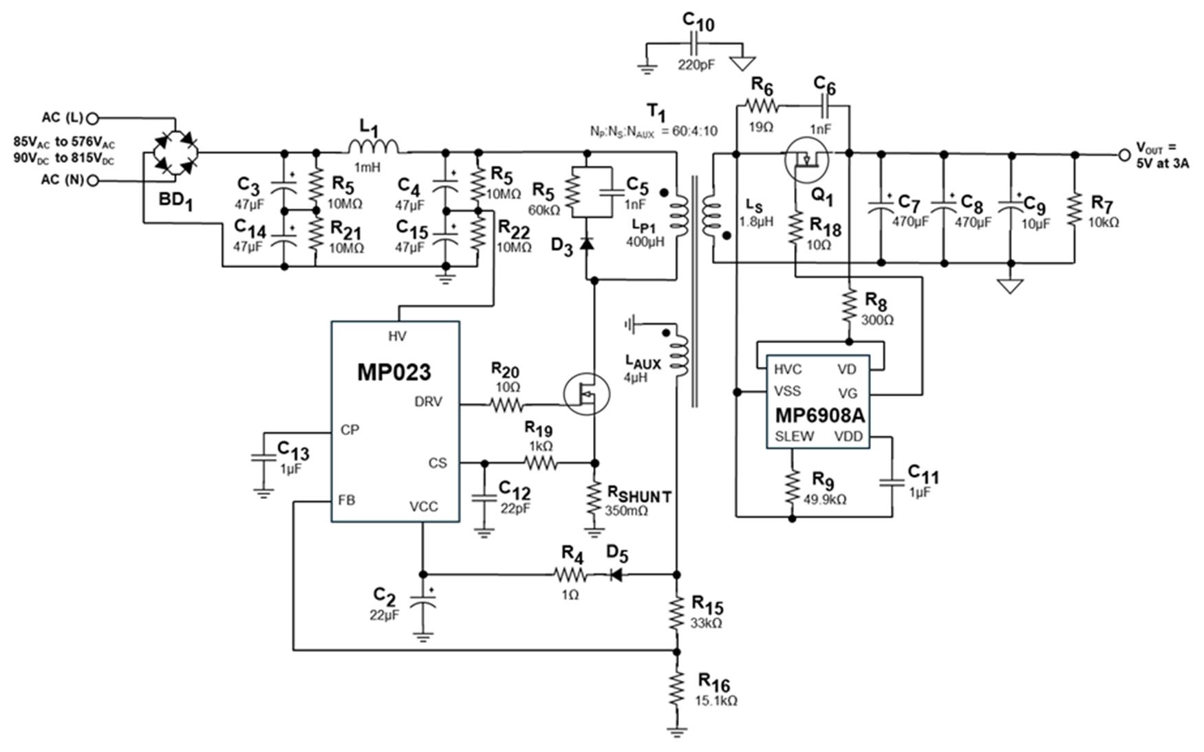
图 4:最终设计电路原理图
实验结果
为了验证上述计算,我们搭建出一个具有超宽输入电压范围的反激式变压器原型(见图 5)。
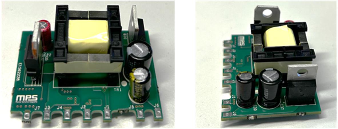
图 5:具有超宽输入电压范围的反激式变换器原型(无输入滤波器的 PCB)
该原型没有配置输入滤波器,这样可以使PCB更加灵活,它可以插入配置了不同输入滤波元件的另一个 PCB。
图 6 显示了变换器在最小电压下的验证结果。蓝色迹线代表原边 MOSFET 的漏源电压(VDS),粉色迹线代表通过分流电阻采样得到的原边电流。
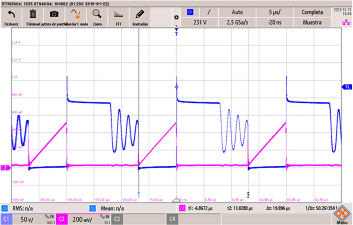
图 6:最小输入电压下的变换器验证结果
图 7 显示了最大电压下的变换器验证结果。蓝色轨迹代表原边 MOSFET 的漏源电压(VDS)。
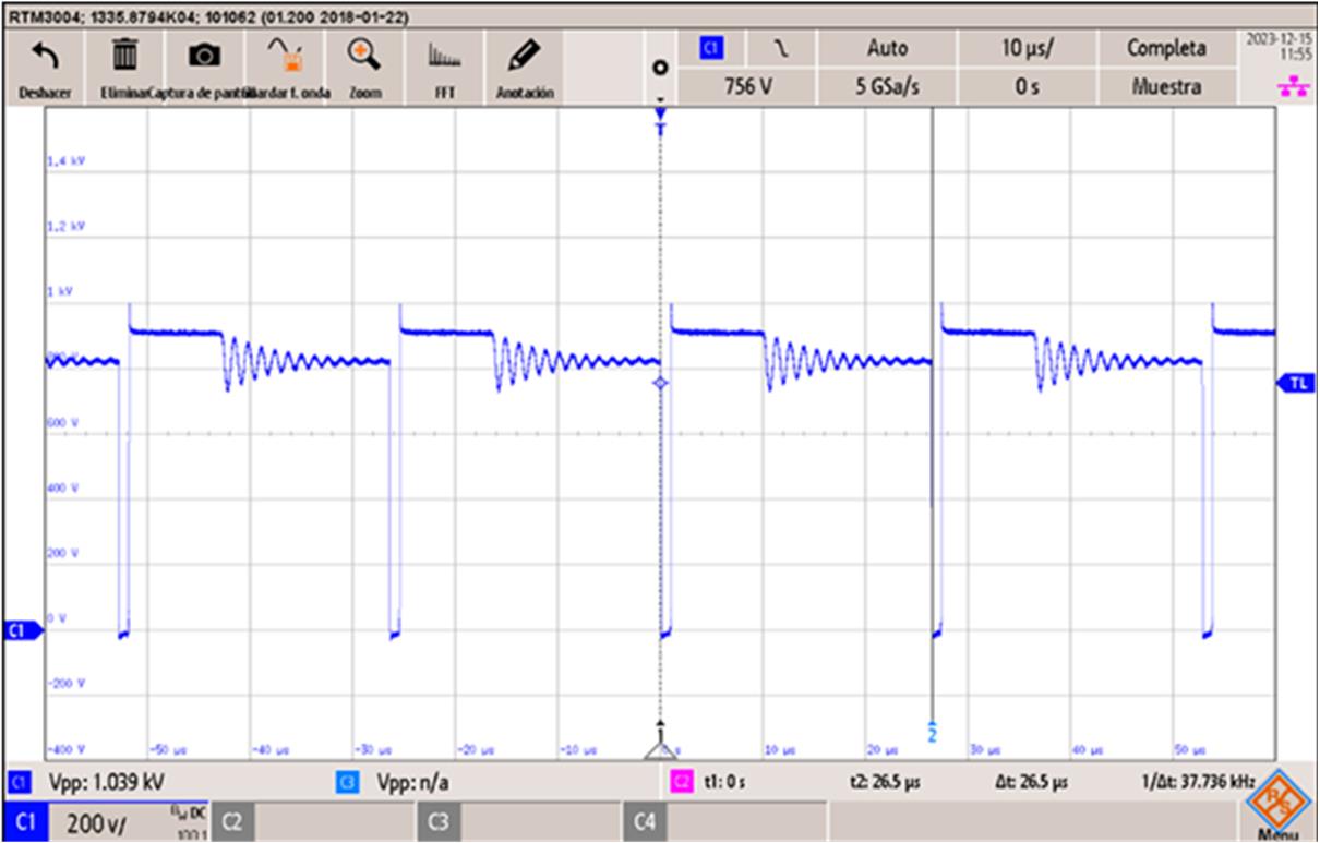
图 7:最大输入电压下的变换器验证结果
图 8 显示了本设计在不同输入电压下的效率验证结果。
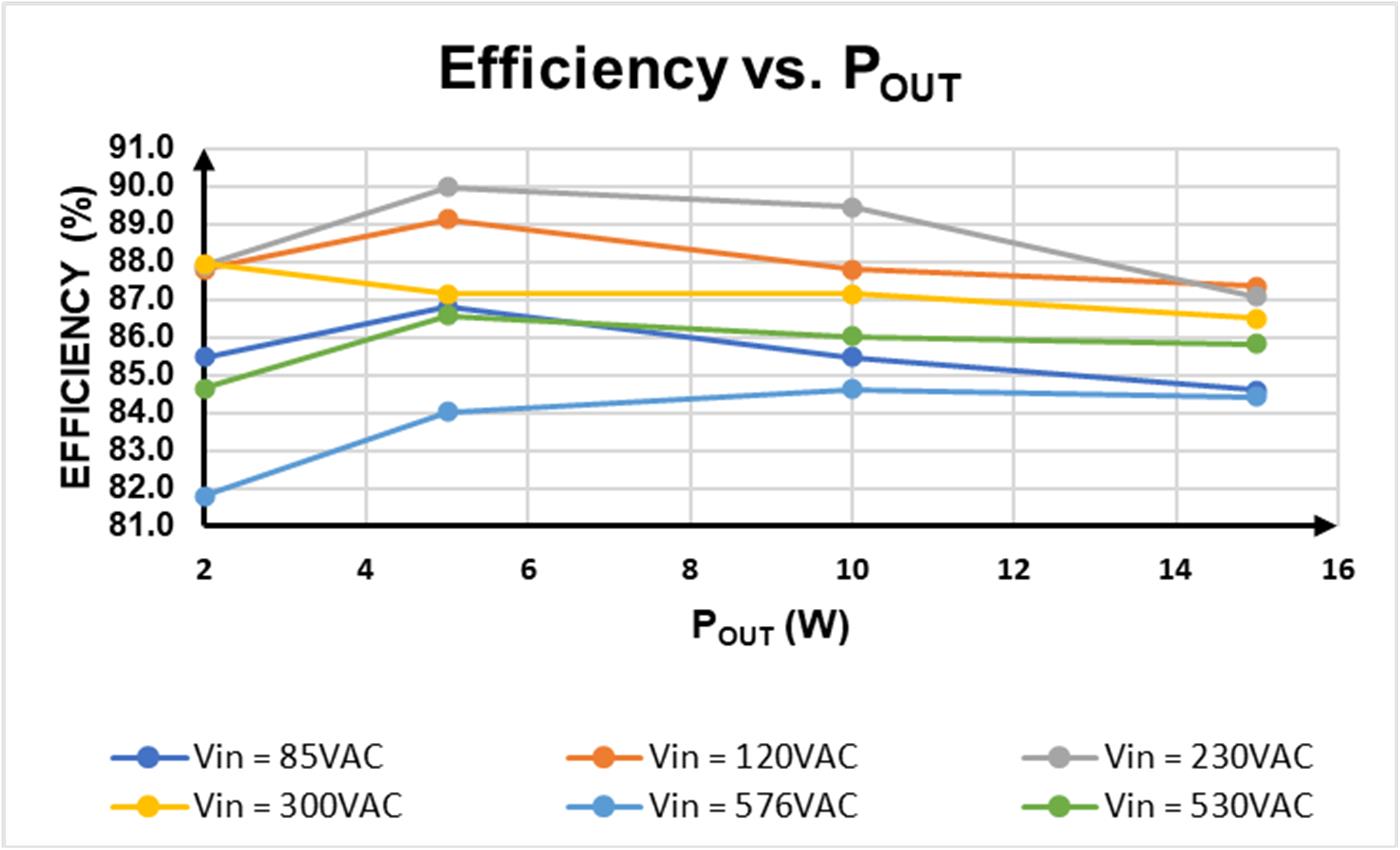
图 8:效率验证结果
如上图所示,由于副边采用了同步整流,变换器的效率相当高。此外,采用具有相对较低栅极电荷电容的原边 MOSFET 还可以降低高VIN下的开关损耗。
结语
在需要三相输入的众多工业应用中,具有宽VIN范围的反激式变换器非常有用。本文提供了一系列简单步骤,可通过MP023优化反激式变换器的设计。这些步骤包括了计算所需的匝数比、磁化电感和分流电阻,还包括选择关键参数以优化原边和副边 MOSFET 的设计。文中同时提供了设计验证结果,以证明本文所述方法的一致性和可行性。
除了 MP023 之外,MPS 还提供多款具有原边调节功能的反激式变换器。立即了解 MPS 强大的产品组合,找到满足您设计需求的解决方案。
_______________________
您感兴趣吗?点击订阅,我们将每月为您发送最具价值的资讯!
技术论坛
 Latest activity 3 years ago
 9 回复
Latest activity 3 years ago
3 回复
Latest activity 4 months ago
9 回复
9 回复
Latest activity 3 years ago
3 回复
Latest activity 4 months ago
9 回复
直接登录
创建新帐号