How to Design a Feedback Loop Compensator for a Flyback Converter in Four Steps

Get valuable resources straight to your inbox - sent out once per month
We value your privacy
Introduction
Due to their versatility, ease of design, and low cost, flyback converters have become one of the most widely used topologies in power electronics. Its structure derives from one of the three basic topologies — specifically, buck-boost topology. However, unlike buck-boost converters, flyback topologies allow the voltage output to be electrically isolated from the input power supply. This feature is vital for industrial and consumer applications.
Among the different control methods used to stabilize power converters, the most widely used control method is peak current mode, which continuously senses the primary current to provide important protection for the power supply. Additionally, to obtain a higher design performance, it is common to regulate the converter with the output that has the highest load using a technique called cross-regulation.
This article aims to show readers, engineers, and students how to correctly design the control loop that stabilizes the flyback converter in order to provide optimal functionality. This process includes minimizing the stationary error, increasing/decreasing the bandwidth as required, and increasing the phase/gain margin as much as possible.
Closed-Loop Flyback Converter Block Diagram
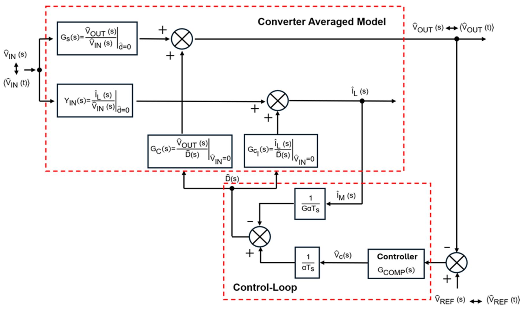
Before making the necessary calculations for the controller to stabilize the peak current control mode flyback, it is important to understand the components of the entire closed-loop system: the converter averaged model and the control loop (see Figure 1).

Figure 1: Closed-Loop System Block Diagram
The design engineer’s main interest is to study the behavior of the converter under load changes. Considering a fixed input voltage (VIN), the open-loop transfer function can be modeled under small perturbations produced in the duty cycle to study the power supply’s dynamic response.
The summarized open-loop system can be modeled with Equation (1):
$$ T_{V0}(s) = \left. \frac{\hat{V}_{OUT}(s)}{\hat{V}_{C}(s)} \right|_{\hat{V}_{IN} = 0} = \frac{G \cdot G_{C}(s)}{G_{CI}(s) + G\alpha T_{s}} $$Where G is the current-sense gain transformed to voltage, GC(s) and GCI(s) are the transfer functions of the flyback converter in terms of output voltage and magnetizing current response (respectively) under small perturbations in the duty cycle, and GαTS is the modelling of the ramp compensation to avoid the double-pole oscillation at half of the switching frequency.
Flyback Converter Control Design and Component Selection
There are many decisions and tradeoffs involved in designing the flyback converter’s control loop. The following sections of the article will explain the design process step by step.
Figure 2 shows the design flow.
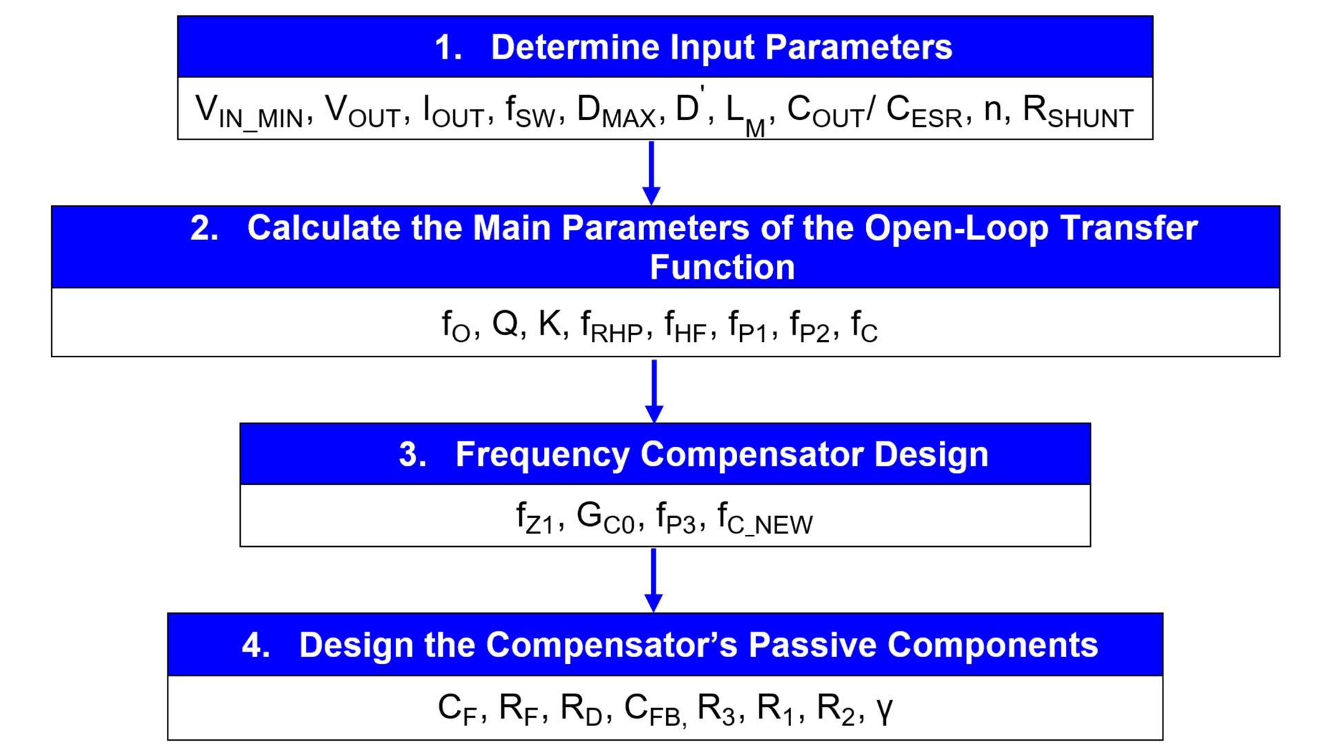
Figure 2: Control Loop Design Flowchart
Control Loop Design Process and Calculations
Step 1: Design Inputs
Once the converter’s main parameters have been designed according to the relevant specifications, it is time to define the parameters as inputs for the control loop design. These parameters include the input and output voltages (VIN and VOUT, respectively), operation mode, switching frequency (fSW), duty cycle, magnetizing inductance (LM), turns ratio (NP:NS), shunt resistor (RSHUNT), and output capacitance (COUT). Table 1 shows a summary of the design inputs for the circuit discussed in this article.
Table 1: Summary of Design Inputs
| Design Input | Value |
| Minimum input voltage (VIN_MIN) | 85VAC |
| Output voltage (VOUT) | 12V |
| Output current (IOUT) | 3.33A |
| Operation mode | CCM at VIN_MIN |
| Switching frequency (fSW) | 65kHz |
| Maximum duty cycle (DMAX) | 46% |
| Secondary duty cycle (D’) | 54% |
| Magnetizing inductance (LM) | 610µH |
| Output capacitance/ESR (COUT/CESR) | 950µF/15mΩ |
| Turns ratio NS:NP (n) | 1/6 |
| Shunt resistor (RSHUNT) | 0.4Ω |
To design a flyback converter compensator, it is necessary to first obtain all main components that make the converter. For this article, MPS’s HF500-40 flyback regulator will be used to demonstrate that designing a compensator using optocoupler feedback is not a complex process. This device is a fixed-frequency, current-mode regulator with built-in slope compensation. Because the converter works in continuous conduction mode (CCM) at low line input, a double-pole oscillation at half of the switching frequency is produced; built-in slope compensation dampens this oscillation, making its effect almost null.
Step 2: Calculate the Parameters of the Open-Loop Transfer Function
It is vital to calculate the parameters of the open-loop transfer function and calculate the values for all of the compensator’s parameters that can optimize the converter at the dynamic behavior level.
The open-loop transfer function of the peak current control flyback converter (also including the compensation ramp factor) can be estimated with Equation (2):

Where D' is defined by the percentage of time that the secondary diode (or synchronous FET) is active during a switching cycle.
The basic canonical model can be defined with Equation (3):
$$ \left. \frac{\hat{V}_{OUT}(s)}{\hat{V}_{C}(s)} \right|_{\hat{V}_{IN} = 0} = G_{C0} \cdot \left(1 - \frac{s}{\omega_{\text{RHP}}} \right) \left(1 + \frac{s}{\omega_{\text{HF}}} \right) \Bigg/ \left[ \left( \frac{s}{\omega_o} \right)^2 + \frac{s}{\omega_o Q} + 1 \right] $$
Note that the equivalent series resistance (ESR) effect on the output capacitors has been included in the transfer function, as it is the most significant parasitic effect.
By using Equation (2) and Equation (3), it is possible to calculate the vital parameters.
The resonant frequency (fO) can be calculated with Equation (4):
$$ f_O = \frac{\omega_0}{2\pi} = \frac{1}{2\pi} \cdot \sqrt{ \frac{ \left( \frac{{D'}^3 \cdot V_{OUT} \cdot T_s \cdot R}{n^2 \cdot L_M} + 2 \cdot n \cdot V_{IN} \cdot (1 + D) \right) }{ R \cdot V_{OUT} \cdot D' \cdot T_s \cdot C_{OUT} } } $$
After inputting the relevant values, fO can be calculated with Equation (5):
$$ f_0 = \frac{1}{2\pi} \sqrt{ \frac{ \left( \frac{0.54^3 \times 12 \times \frac{12}{3.33}}{ \left( \frac{1}{6} \right)^2 \times 610 \times 10^{-6} \times 65 \times 10^3 } + 2 \times \frac{1}{6} \times 85 \sqrt{2} \times (1 + 0.46) \right) }{ \frac{12}{3.33} \times 12 \times 0.54 \times \frac{1}{65 \times 10^3} \times 950 \times 10^{-6} } } = 2.191 \, \text{kHz} $$
The right-half-plane zero (fRHP) can be estimated with Equation (6):
$$ f_{\text{RHP}} = \frac{{D'}^2 \cdot R}{2\pi n^2 L_M D} = \frac{0.54^2 \cdot \frac{12}{3.33}}{2\pi \cdot \left( \frac{1}{6} \right)^2 \cdot 610 \times 10^{-6} \cdot 0.46} = 21.46 \, \text{kHz} $$The q-factor (Q) can be calculated with Equation (7):
$$ Q = \frac{ \sqrt{ \left( \frac{{D'}^3 V_{OUT} T_s R}{n^2 L_M} + 2 n V_{IN} (1 + D) \right) } \cdot \sqrt{ R V_{OUT} D' T_s C_{OUT} } }{ V_{OUT} D' T_s + 2 n C_{OUT} R V_{IN} } $$
After inputting the relevant values, Q can be estimated with Equation (8):
$$ Q = \frac{ \sqrt{ \left( \frac{0.54^3 \cdot 12 \cdot \frac{12}{3.33}}{ \left( \frac{1}{6} \right)^2 \cdot 610 \cdot 10^{-6} \cdot 65 \cdot 10^3 } + 2 \cdot \frac{1}{6} \cdot 85 \sqrt{2} \cdot (1 + 0.46) \right) } \cdot \sqrt{ \frac{12}{3.33} \cdot 12 \cdot 0.54 \cdot \frac{1}{65 \cdot 10^3} \cdot 950 \cdot 10^{-6} } }{ 12 \cdot 0.54 \cdot \frac{1}{65 \cdot 10^3} + 2 \cdot \frac{1}{6} \cdot 950 \cdot 10^{-6} \cdot \frac{12}{3.33} \cdot 85 \sqrt{2} } = 0.034 $$
The DC gain (K) can be calculated with Equation (9):
$$ K = \frac{ 2 \cdot G \cdot V_{\text{IN}} \cdot D' \cdot R }{ \frac{{D'}^3 \cdot V_{\text{OUT}} \cdot T_s \cdot R}{n^2 \cdot L_M} + 2 \cdot n \cdot V_{\text{IN}} \cdot (1 + D) } $$where
$$ G = \frac{1}{R_{\text{SHUNT}}} $$After inputting the relevant values, K can be estimated with Equation (10):
$$ K = \frac{ 2 \cdot \frac{1}{0.4} \cdot 85 \sqrt{2} \cdot 0.54 \cdot \frac{12}{3.33} }{ \frac{ 0.54^3 \cdot 12 \cdot \frac{12}{3.33} }{ \left( \frac{1}{6} \right)^2 \cdot 610 \times 10^{-6} \cdot 65 \times 10^3 } + 2 \cdot \frac{1}{6} \cdot 85 \sqrt{2} \cdot (1 + 0.46) } = 18.08 = 25.14\,\text{dB} $$The high-frequency zero (fHF) can be calculated with Equation (11):
$$ f_{\text{HF}} = \frac{1}{2\pi C_{OUT} R_{ESR}} = \frac{1}{2\pi \cdot 950 \times 10^{-6} \cdot 15 \times 10^{-3}} = 16.75\,\text{kHz} $$It is important to note that with current mode control, it is common to obtain values well below 0.5 for Q. With this in mind, the result of the second-degree polynomial in the denominator of the transfer function ends up giving two real and negative poles. This is different from voltage-control mode or when there is a very large compensation ramp, which results in two complex conjugate poles.
The two real and negative poles can be estimated with Equation (12):
$$ f_{P1} = Q \cdot f_O = 0.034 \times 2191 = 74.5\,\text{Hz} \quad \text{and} \quad f_{P2} = \frac{f_O}{Q} = \frac{2191}{0.034} = 64.44\,\text{kHz} $$The new open-loop transfer function can be calculated with Equation (13):
$$ \left. \frac{\hat{V}_O(s)}{\hat{V}_C(s)} \right|_{\hat{V}_g = 0} = K \cdot \frac{ \left(1 - \frac{s}{\omega_{\text{RHP}}} \right) \left(1 + \frac{s}{\omega_{\text{HF}}} \right) }{ \left(1 + \frac{s}{\omega_{p1}} \right) \left(1 + \frac{s}{\omega_{p2}} \right) } = 25.14 \cdot \frac{ \left(1 - \frac{s}{2\pi \cdot 21.46 \cdot 10^3} \right) \left(1 + \frac{s}{2\pi \cdot 16.75 \cdot 10^3} \right) }{ \left(1 + \frac{s}{2\pi \cdot 74.5} \right) \left(1 + \frac{s}{2\pi \cdot 64.44 \cdot 10^3} \right) } $$The cutoff frequency (fC) can be estimated with Equation (14): $$ f_C = f_{P1} \cdot K = 74.5 \times 18.08 = 1.35\,\text{kHz} $$
The following sections will explain how the frequency compensator design achieves power supply stability and excellent performance.
Step 3: Frequency Compensator Design
Once the open-loop transfer function is modelled, it is necessary to design the frequency compensator such that it achieves the best performance possible. Because the frequency response of the above transfer function has two separate poles (one at a low frequency and one at a high frequency), a simple Type II compensator can be designed. This compensator does not need an additional zero, which is not the case in voltage-control mode because there is a double pole that produces a resonance.
To minimize the steady-state error, it is necessary to design an inverted-zero (or a pole at the origin) because it produces higher gains at low frequencies. To ensure that the system’s stability is not impacted, the frequency must be at least 10 times lower than the first pole, calculated with Equation (15):
$$ f_{Z1} \leq \frac{f_{P1}}{10} \;\Rightarrow\; f_{Z1} \leq \frac{74.5}{10} \;\Rightarrow\; f_{Z1} \leq 7.45\,\text{Hz} $$Due to the ESR parasitic effect at high frequencies, it is necessary to design a high-frequency pole to compensate for and remove this effect. The pole can be estimated with Equation (16):
$$ f_{P3} \approx f_{HF} \;\Rightarrow\; f_{P3} \approx 16.75\,\text{kHz} $$On the other hand, it is common to modify the cutoff frequency to achieve a higher or lower bandwidth and produce faster or slower dynamic responses, respectively. Once the cutoff frequency is selected (in this case, fC is increased up to 6.5kHz, or 10% of fSW), then the compensator’s middle-frequency gain can be calculated with Equation (17):
$$ G_{\text{COMP}} = \frac{f_{C,\text{NEW}}}{f_{P1}} \cdot \frac{1}{K} \cdot \frac{ \sqrt{1 + \left( \frac{\omega_{z1}}{\omega_{C,\text{NEW}}} \right)^2} }{ \sqrt{1 + \left( \frac{\omega_{C,\text{NEW}}}{\omega_{P3}} \right)^2} } = \frac{6.5 \times 10^3}{74.5} \cdot \frac{1}{18.08} \cdot \frac{ \sqrt{1 + \left( \frac{2\pi \cdot 7.45}{2\pi \cdot 6.5 \times 10^3} \right)^2} }{ \sqrt{1 + \left( \frac{2\pi \cdot 6.5 \times 10^3}{2\pi \cdot 16.75 \times 10^3} \right)^2} } = 4.5 = 13.06\,\text{dB} $$Once the compensator has been designed within the frequency range, calculate the values of the passive components.
Step 4: Design the Compensator’s Passive Components
The most common Type II compensator used for stabilization in current control mode flyback converters with cross-regulation is made up of an optocoupler feedback (see Figure 3).
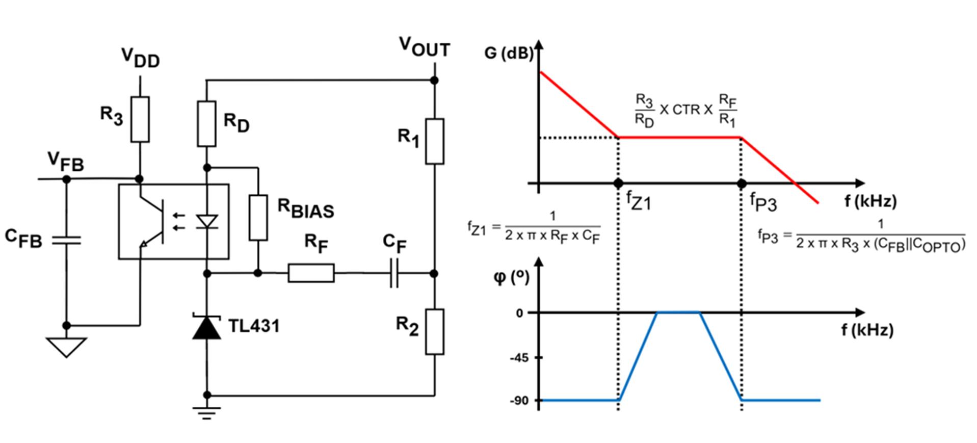
Figure 3: Type-II Compensator Made Up with Optocoupler Feedback
The compensator transfer function based on optocoupler feedback can be estimated with Equation (18):
$$ G_{\text{COMP}}(s) = - \frac{R_3}{R_D} \cdot \text{CTR} \cdot \frac{R_F}{R_1} \cdot \frac{1 + R_F C_F s}{s \left[ R_3 \left( C_{\text{FB}} \parallel C_{\text{OPTO}} \right) s + 1 \right]} $$The middle-frequency gain is formed by two stages: the optocoupler gain and the adjustable voltage reference compensator gain, calculated with Equation (19):
$$ \left\| G_{\text{COMP}} \right\| = \frac{R_3}{R_D} \cdot \text{CTR} \cdot \frac{R_F}{R_1} $$It is important to calculate the maximum resistance to correctly bias the optocoupler. This resistance can be estimated with Equation (20):
$$ R_D \leq \frac{ \left( V_{OUT} - V_F - V_{\text{DZ1,MIN}} \right) \cdot R_3 \cdot \text{CTR}_{\text{MIN}} }{ V_{DD} - V_{\text{CE,SAT}} + \text{CTR}_{\text{MIN}} \cdot R_3 \cdot I_{\text{BIAS}} } $$The parameters necessary to calculate RD can be found in the optocoupler and the adjustable voltage reference datasheets. Table 2 shows the typical values for these parameters from the optocoupler.
Table 2: Main Optocoupler Parameters
| Input Parameters | Value |
| Forward voltage (VF) | 1V |
| Bias current (IBIAS) | 1mA |
| Optocoupler minimum current transfer ratio (CTRMIN) | 0.3 |
| Optocoupler nominal current transfer ratio (CTR) | 1 |
| Collector-emitter saturation voltage (VCE_SAT) | 0.2V |
| Optocoupler output capacitance (COPTO) | 200pF |
Table 3 shows the typical values for these parameters from the adjustable voltage reference.
Table 3: Adjustable Voltage Reference Parameters
| Input Parameters | Value |
| Minimum reference voltage (VDZ1_MIN) | 2.495V |
| Feedback resistor (R1) | 100kΩ |
| Feedback resistor (R2) | 26.3kΩ |
| Maximum VFB | 3.9V |
Once the above parameters have been obtained, RD can be calculated with Equation (21):
$$ R_D \leq \frac{ \left( V_{OUT} - V_F - V_{\text{DZ1,MIN}} \right) \cdot R_3 \cdot \text{CTR}_{\text{MIN}} }{ V_{DD} - V_{\text{CE,SAT}} + \text{CTR}_{\text{MIN}} \cdot R_3 \cdot I_{\text{BIAS}} } \leq \frac{ (12 - 1 - 2.495) \cdot 12 \times 10^3 \cdot 0.3 }{ 3.9 - 0.2 + 0.3 \cdot 12 \times 10^3 \cdot 1 \times 10^{-3} } \leq 4.2\,\text{k}\Omega $$Once the value of R3 is obtained (in this case, R3 is internal to the HF500-40 controller, with a minimum value of 12kΩ), as well as the values for R1, R2, and RD (where RD = 2kΩ), then RF can be estimated with Equation (22):
$$ R_F = \frac{G_{\text{COMP}}}{\dfrac{R_3}{R_D} \cdot \text{CTR}_{\text{NOM}}} \cdot R_1 = \frac{4.5}{\left( \dfrac{12 \times 10^3}{2 \times 10^3} \cdot 1 \right)} \cdot 100 \times 10^3 = 75\,\text{k}\Omega $$Where GCOMP is the compensator’s middle frequency gain, calculated with Equation (17). GCOMP is used to adjust the power supply's bandwidth.
Because the inverted zero and high-frequency pole were already calculated, CF and CFB can be calculated with Equation (23) and Equation (24), respectively:
(23)
$$ f_{z1} = \frac{1}{2\pi R_F C_F} \;\Rightarrow\; C_F = \frac{1}{2\pi R_F f_{z1}} = \frac{1}{2\pi \cdot 75 \times 10^3 \cdot 7.45} = 285\,\text{nF} $$(24)
$$ f_{P3} = \frac{1}{2\pi R_3 (C_{\text{FB}} \parallel C_{\text{OPTO}})} \;\Rightarrow\; C_{\text{FB}} = \frac{1}{2\pi f_{P3} R_3} - C_{\text{OPTO}} = \frac{1}{2\pi \cdot 16.75 \times 10^3 \cdot 12 \times 10^3} - 200 \times 10^{-12} = 592\,\text{pF} $$Once the open-loop system and compensator have been designed, the loop gain transfer function can be estimated with Equation (25):
$$ G_{\text{TOTAL}}(s) = 38.2 \cdot \frac{ \left(1 - \frac{s}{2\pi \cdot 21.46 \times 10^3} \right) \left(1 + \frac{s}{2\pi \cdot 16.75 \times 10^3} \right) }{ \left(1 + \frac{s}{2\pi \cdot 74.5} \right) \left(1 + \frac{s}{2\pi \cdot 64.44 \times 10^3} \right) } \cdot \frac{ \left(1 + \frac{s}{2\pi \cdot 7.45} \right) }{ s \cdot \left( \frac{s}{2\pi \cdot 16.75 \times 10^3} + 1 \right) } $$Equation (25) is based on Equation (13) and Equation (18).
It is important to calculate the phase and gain margins to ensure the stability of the power supply.
The phase margin can be calculated with Equation (26):
$$ \gamma = 180^\circ - \tan^{-1} \left( \frac{\omega_{C,\text{NEW}}}{\omega_{\text{RHP}}} \right) - \tan^{-1} \left( \frac{\omega_{z1}}{\omega_{C,\text{NEW}}} \right) + \tan^{-1} \left( \frac{\omega_{C,\text{NEW}}}{\omega_{\text{HF}}} \right) - \tan^{-1} \left( \frac{\omega_{C,\text{NEW}}}{\omega_{P1}} \right) - \tan^{-1} \left( \frac{\omega_{C,\text{NEW}}}{\omega_{P2}} \right) - \tan^{-1} \left( \frac{\omega_{C,\text{NEW}}}{\omega_{P3}} \right) $$After inputting the relevant values, the phase margin can be calculated with Equation (27):
$$ \gamma = 180^\circ - \tan^{-1} \left( \frac{6.5 \times 10^3}{21.46 \times 10^3} \right) - \tan^{-1} \left( \frac{7.45}{6.5 \times 10^3} \right) + \tan^{-1} \left( \frac{6.5 \times 10^3}{16.75 \times 10^3} \right) - \tan^{-1} \left( \frac{6.5 \times 10^3}{74.5} \right) - \tan^{-1} \left( \frac{6.5 \times 10^3}{64.44 \times 10^3} \right) - \tan^{-1} \left( \frac{6.5 \times 10^3}{16.75 \times 10^3} \right) = 68^\circ $$If the phase margin exceeds 50°, it is an important parameter necessary to comply with certain standards.
At the same time, the gain margin can be approximated with Equation (28):
$$ \gamma = 180^\circ - \tan^{-1} \left( \frac{\omega}{21.46 \times 10^3} \right) - \tan^{-1} \left( \frac{7.45}{\omega} \right) + \tan^{-1} \left( \frac{\omega}{16.75 \times 10^3} \right) - \tan^{-1} \left( \frac{\omega}{74.5} \right) - $$ $$ \tan^{-1} \left( \frac{\omega}{66.44 \times 10^3} \right) - \tan^{-1} \left( \frac{\omega}{16.75 \times 10^3} \right) = 0^\circ \;\Rightarrow\; \omega = 37.84\,\text{kHz} $$Equation (29) is derived from Equation (25) at the specified frequency:
$$ \left\| G_{\text{TOTAL}}(s) \right\| = 10^{\frac{38.2}{20}} \cdot \frac{ \sqrt{1 + \left( \frac{2\pi \cdot 37.84 \times 10^3}{2\pi \cdot 21.46 \times 10^3} \right)^2} \cdot \sqrt{1 + \left( \frac{2\pi \cdot 37.84 \times 10^3}{2\pi \cdot 16.75 \times 10^3} \right)^2} }{ \sqrt{1 + \left( \frac{2\pi \cdot 37.84 \times 10^3}{2\pi \cdot 74.5} \right)^2} \cdot \sqrt{1 + \left( \frac{2\pi \cdot 37.84 \times 10^3}{2\pi \cdot 66.44 \times 10^3} \right)^2} } \cdot \frac{ \sqrt{1 + \left( \frac{2\pi \cdot 7.5}{2\pi \cdot 37.84 \times 10^3} \right)^2} }{ \sqrt{1 + \left( \frac{2\pi \cdot 37.84 \times 10^3}{2\pi \cdot 16.75 \times 10^3} \right)^2} } $$ $$ \left\| G_{\text{TOTAL}}(s) \right\| = 0.282 \;\Rightarrow\; \left\| G_{\text{TOTAL}}(s) \right\|_{\text{dB}} = -11\,\text{dB} $$In this scenario, the gain margin is below -10dB, which is another important parameter to consider, particularly in regards to compliance with regulation specifications. If the result is close to 0dB, some iteration is necessary to decrease the value; otherwise, the performance is suboptimal. This iteration must start by decreasing the value of the cutoff frequency.
This complete transfer function provides stability to the power supply and the best performance as possible by:
- Minimizing steady-state error.
- Minimizing the ESR parasitic effect.
- Increasing the bandwidth of the power supply up to 6.5kHz.
Final Design
After calculating all of the passive component values for the feedback loop compensator and determining the converter’s main parameters, the entire flyback can be designed using the HF500-40. Figure 4 shows the circuit’s final design using all calculated parameters.
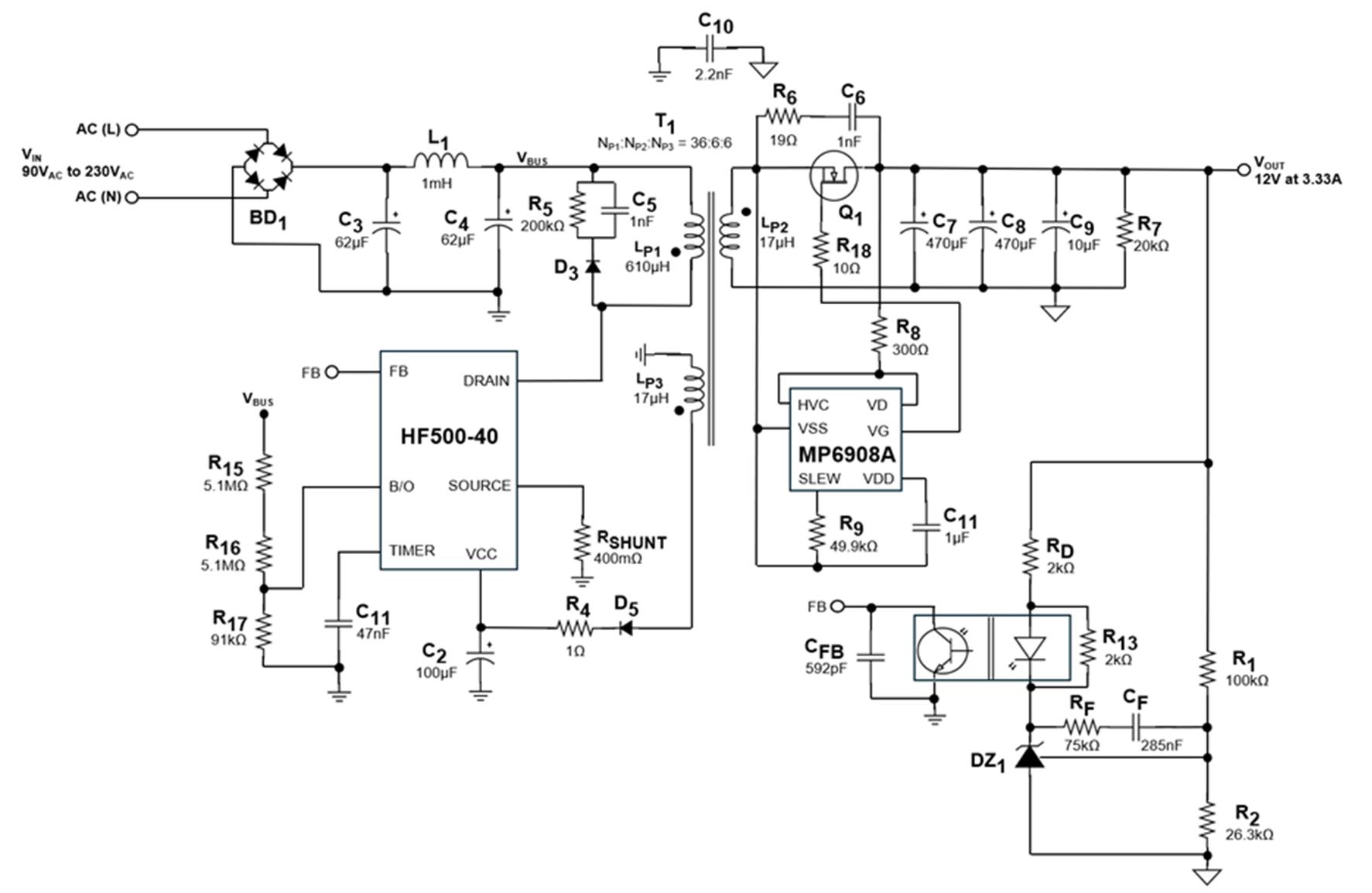
Figure 4: Final Design Circuit Schematic
Figure 5 shows the bode plot of the complete loop gain frequency response.
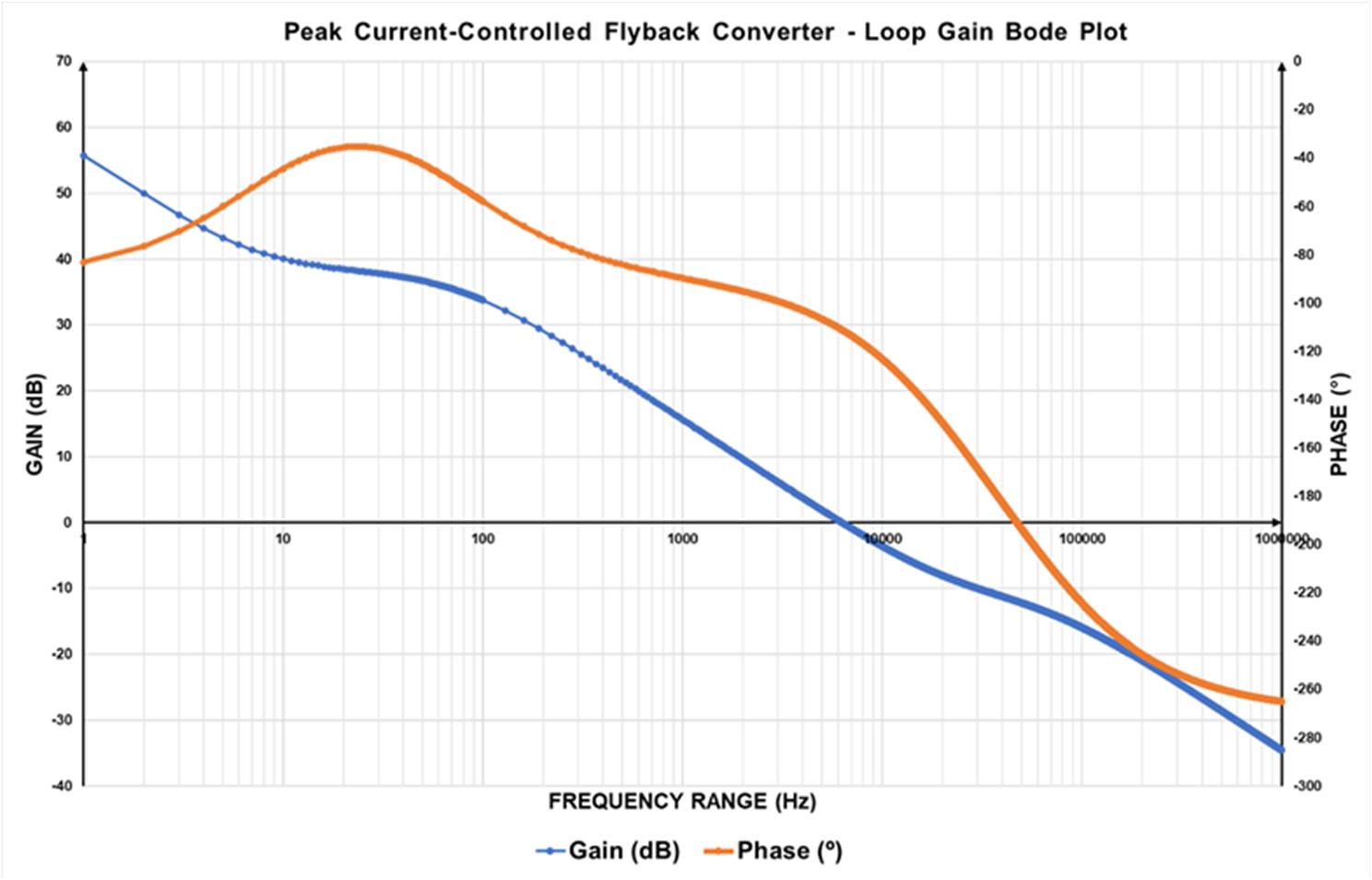
Figure 5: Bode Plot of the Complete Loop Gain Frequency Response
Conclusion
Obtaining the flyback averaged model via small-signal analysis is a complex process to most accurately approximation of the converter’s transfer functions. In addition, the cross-regulation technique involves secondary-side regulation through optocoupler feedback and an adjustable voltage reference, which complicates calculations.
However, by following the four steps explained in this article, a good approximation can be obtained to improve the power supply’s performance, as the output with the heaviest load is directly regulated. This means that the output can react quickly to load changes. Thus, designing an optocoupler feedback compensator using the HF500-40 is not a complex process. Explore MPS’s secondary-side regulation solutions to optimize your flyback topology design.
_______________________
Did you find this interesting? Get valuable resources straight to your inbox - sent out once per month!
技术论坛
 Latest activity 2 years ago
 9 回复
9 回复
 Latest activity 2 years ago
 3 回复
3 回复
 Latest activity 9 months ago
 6 回复
6 回复




直接登录
创建新帐号