Introduction and Principle of Operation
The buck converter, also referred to as a step-down converter, is a popular topology in power electronics that converts a higher input voltage to a lower output voltage. It is crucial in various applications, from portable devices to automotive systems, where specific components or subsystems require a lower voltage level to operate. The primary advantage of the buck converter is its simplicity, which enables efficient voltage conversion using a relatively small number of components.
The operating principle of the buck converter involves controlled energy transfer from the input to the output through switches, an inductor, and a capacitor. A high-side switch (usually a MOSFET) and a low-side switch (typically a diode) are employed in the buck converter to control the current flow through the inductor. By adjusting the duty cycle of the high-side switch, the average output voltage can be regulated proportionally to the input voltage.
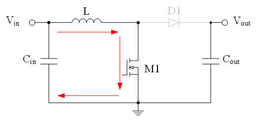
When the high-side switch of a buck converter is switched on, it allows current to flow through the inductor, which stores energy in its magnetic field. This stored energy is then transferred to the output, charging the output capacitor and powering the load. When the high-side switch is turned off and the low-side switch is turned on, the inductor's magnetic field collapses, releasing the stored energy and maintaining the current flow to the load. The buck converter is designed to operate within a closed-loop control system, where a feedback mechanism continuously compares the output voltage to a reference voltage to ensure that the output voltage remains stable and regulated, regardless of changes in input voltage or load conditions.
Circuit Topology and Key Components
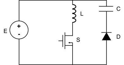
Figure 1 shows the circuit diagram of the buck converter, which consists of a source of DC power supply E, a switch S (typically a MOSFET or IGBT), a diode D, low frequency bandpass LC filter and load R. The transistor is represented by a switch S with a small arrow, which marks the direction of the current that can be established through the switch.

Figure 1: The Buck Converter Circuit Diagram
When the switch S is turned on, the diode D becomes inversely polarized by the supply voltage E, and the voltage across the inductor becomes equal to the difference between the supply voltage and the load voltage (see Figure 2):
$$u_L=E-U$$The current flowing through the inductor will increase linearly from the minimum to the maximum value (see Figure 3).

Figure 2: The Buck Converter Circuit Diagram – Interval tON
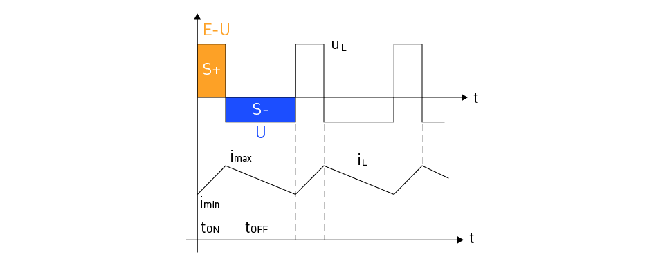
Figure 3: The Buck Converter – Inductor Voltage and Current Versus Time Graph
When the switch S is turned off, the commutation process occurs in which the inductor’s current from the source E passes into the diode D. This process is shown in Figure 4. For better understanding the commutation process, it is necessary to take into account that the inductor’s winding consists of a series of coils located next to each other, so that there is not only magnetic coupling between them but also capacitive coupling, which is represented by the capacitor CP. The moment before switching off (the switch S), the voltage across the inductor was
$$u_L=u_{Cp}=E-U$$After the switch S is turned off, the current through the inductor remains the same in direction and intensity and closes through the capacitor CP (see Figure 4-a). In the next period, the capacitor discharges and charges to the other side. The reverse voltage of the diode is
$$u_{Dr}=U+u_L=U+u_{Cp}$$and becomes zero when the voltage across the capacitor CP becomes equal to the load voltage in the opposite direction. At that moment, the diode takes over the inductor's current (see Figure 4-b), so the voltage across the inductor is equal to the load voltage
$$u_L=-U$$and the current through the inductor linearly decreases and reaches a minimum value at the end of the period (see Figure 3).

Figure 4: The Buck Converter Circuit Diagram - Interval tOFF
In steady state, over one switching cycle, the total change in inductor current is equal to zero:
$$\Delta I_L = \frac{1}{L} \int_{0}^{T} u_L dt = 0 \Rightarrow \int_{0}^{T} u_L dt = 0$$This implies that in steady state, the area of the voltage waveform across the inductor is equal to zero, that is:
$$S_+ = S_- \Rightarrow (E - U) \cdot t_{ON} = U \cdot t_{OFF}$$The average load voltage (the voltage across the resistor R) value is equal to:
$$U = E \cdot \frac{t_{ON}}{t_{ON} + t_{OFF}} = E \cdot \frac{ t_{ON}}{T} = E \cdot d$$where d represents the duty cycle of the switch S.
Buck converters employ a simple yet effective circuit topology to step down the input voltage to a lower output voltage. The key components of a buck converter are as follows:
- The high-side switch is a controlled semiconductor device that connects and disconnects the input voltage source to the rest of the circuit. It is usually a MOSFET or IGBT that is controlled by a pulse-width modulation (PWM) signal to determine the duty cycle and output voltage.
- The low-side switch is another electronic device that ensures the current flows through the inductor in the appropriate direction. In non-synchronous buck converters, it is usually a diode, and in synchronous buck converters, it is typically a MOSFET. It is also controlled by a PWM signal, but with a phase difference to complement the operation of the high-side switch.
- The inductor serves as an energy storage element that helps smooth the current waveform and maintain continuous current flow in the circuit. The inductor value is carefully chosen to ensure the desired conduction mode (continuous or discontinuous) and minimize output voltage ripple.
- The output capacitor filters the voltage waveform to reduce voltage ripple and provide a stable output voltage for the load. The capacitance value, equivalent series resistance (ESR), and equivalent series inductance (ESL) all play a significant role in determining the converter's performance and the quality of the output voltage.
- The control circuitry generates the PWM signals to drive the high- and low-side switches monitors the output voltage, and adjusts the duty cycle to regulate voltage. The control circuitry may use various feedback mechanisms, such as voltage-mode control, current-mode control, or advanced control strategies to optimize the converter's performance and stability.
These components, together with some additional passive components (such as input capacitors and resistors for feedback networks), form the basic circuit topology of a buck converter. By properly selecting and designing these components, a buck converter can efficiently and effectively step down the input voltage to the desired output voltage for various applications.
Continuous and Discontinuous Conduction Modes
In buck converters, the flow of current through the inductor can be described by two distinct conduction modes: continuous conduction mode (CCM) and discontinuous conduction mode (DCM). Understanding these modes is essential for properly designing and analyzing the converter.
Continuous Conduction Mode (CCM): In this mode, the current flowing through the inductor never drops to zero during the entire switching cycle. This mode ensures that the inductor continuously stores and releases energy throughout the cycle, while the output voltage is primarily determined by the high-side switch duty cycle and input voltage. Although CCM is often preferred because it offers lower output voltage ripple, smaller filter components, and reduced stress on switches, it requires more complex control schemes to maintain stability under varying load conditions.
Discontinuous Conduction Mode (DCM): In DCM, the current through the inductor falls to zero for a portion of the switching cycle when the load current is lower than the average inductor current. This results in the inductor fully discharging its stored energy before the next cycle begins, leading to higher output voltage ripple and increased EMI due to abrupt changes in current flow. However, DCM offers benefits such as improved light-load efficiency, simpler control schemes, and reduced reverse-recovery losses in the low-side diode.
Choosing between CCM and DCM: The choice of conduction mode depends on the specific application requirements, such as load current range, output voltage ripple tolerance, and efficiency targets. Designers must carefully consider these factors and select the appropriate conduction mode for their buck converter design.
In some cases, a converter may operate in CCM under heavy-load conditions and transition to DCM under light-load conditions. This behavior, known as boundary conduction mode (BCM) or critical conduction mode (CrCM), can benefit both conduction modes, such as high efficiency across a wide load range and reduced component stress. However, it also introduces additional design challenges and may require more complex control schemes to ensure stable operation.
Design Consideration and Calculations
A buck converter's design must take into account a number of crucial factors and computations to guarantee peak performance, efficacy, and dependability. In this section, we'll go over the main aspects that affect buck converter design as well as the calculations that must be done.
Input and output specifications: The first stage in creating a buck converter is to provide the required output current (Iout), desired output voltage (Vout), and input voltage range (Vin_min and Vin_max). The operational parameters of the converter will be chosen in accordance with these specifications.
Duty cycle and switching frequency: The duty cycle (D) is the percentage of the whole switching period when the high-side switch is ON. It is a crucial variable that impacts the output voltage and converter efficiency . The duty cycle can be calculated as follows:
$$D = \frac{V_{out}}{V_{in}}$$The switching frequency (fs) is another essential parameter that influences the size of the inductor and capacitors and the converter's transient response, efficiency, and electromagnetic compatibility (EMC). Higher switching frequencies allow for smaller passive components but may result in higher switching losses and reduced efficiency.
Inductor selection: The inductor is a crucial component in a buck converter, as it stores and releases energy during the switching cycle. The inductor value (L) must be chosen to balance the trade-offs between output voltage ripple, transient response, and size. The required inductor value can be calculated using the following formula:
$$L = \frac{(V_{in} - V_{out}) \cdot D \cdot T}{\Delta I_L}$$Where T is the switching period (1/fs), and ΔIL is the desired inductor current ripple.
Capacitor selection: The output capacitor (Cout) plays a vital role in filtering the output voltage ripple and maintaining stability in the converter. The value of Cout depends on the desired output voltage ripple (ΔVout), the load current, and the switching frequency. The required output capacitor value can be estimated using the following formula:
$$C_{out} = \frac{I_{out} \cdot D \cdot T}{\Delta V_{out}}$$The output capacitor (Cout) filters the output voltage ripple and maintains stability in the converter. To determine the appropriate value for Cout, we must consider the desired output voltage ripple (ΔVout), the load current (Iout), and the switching frequency (fs).
The output voltage ripple (ΔVout) is mainly due to the inductor current ripple (ΔIL) charging and discharging the output capacitor during the switching cycle. The capacitor current (Ic) can be approximated as follows:
$$I_C \approx \frac{\Delta I_L}{2}$$Considering the relationship between the current and capacitance in the time domain:
$$I_C = C \cdot \frac{dV}{dt}$$Where 'Ic' is the capacitor current, 'C' is the capacitance value, 'dV' is the change in voltage across the capacitor, and 'dt' is the change in time.
Combining these two relationships, we get:
$$\frac{\Delta I_L}{2} \approx C_{out} \cdot \frac{\Delta V_{out}}{T}$$Where 'T' is the switching period (1/fs), and 'ΔVout' is the desired output voltage ripple.
Now, we can rearrange the equation to solve for Cout:
$$C_{out} \approx \frac{\Delta I_L \cdot T}{2 \cdot \Delta V_{out}}$$However, it is important to note that the inductor current ripple (ΔIL) is directly proportional to the load current (Iout) and the duty cycle (D). In practice, a higher load current will lead to a larger inductor current ripple. Thus, we can rewrite the equation for Cout by substituting the proportionality relationship between ΔIL and Iout * D:
$$C_{out} \approx \frac{I_{out} \cdot D \cdot T}{\Delta V_{out}}$$Component selection and thermal considerations: In addition to picking the right inductor and capacitor values, it's crucial to select high- and low-side switches (often MOSFETs) with sufficient voltage and current ratings. To ensure dependable functioning, adequate thermal management techniques should be used, such as heatsinks or thermal vias. These procedures should take into account the power losses in these components.
Control loop design: The buck converter's control loop must also be built to maintain output voltage regulation under a variety of input voltage and load situations. Choosing an appropriate control topology (such as voltage mode, current mode, or digital control) and tuning the loop compensation components for stability and the correct transient response are common steps in this process. In conclusion, careful consideration must be given to a number of parameters while constructing a buck converter, including input/output requirements, duty cycle, switching frequency, component selection, and control loop design. Engineers may design effective and dependable buck converters for a variety of applications by considering these elements and running the relevant calculations. To maximize a buck converter's performance and guarantee reliable operation under a variety of circumstances, it is crucial to understand its efficiency and power losses. In this section, we'll talk about how buck converter efficiency is affected by various variables and look at various power loss sources. Efficiency: The ratio of the output power (Pout) to the input power (Pin) is the definition of a buck converter's efficiency (η). It stands for the proportion of input power that successfully transforms into usable output power. The efficiency of a buck converter can be calculated as follows: In power electronic converters, high efficiency is preferred because it decreases power loss, lessens thermal stress on parts, and enhances overall system performance. Depending on the component choice and operating circumstances, typical buck converters can attain efficiencies of 90% or greater. Conduction losses: Conduction losses happen when power is lost because conducting parts, including an inductor, MOSFETs, and a diode, is resistive. In general, these losses are more substantial at larger output currents and grow linearly with the load current. It is essential to choose low-resistance components and design the converter's layout for the least amount of parasitic resistance to reduce conduction losses. Switching losses: Switching losses are caused by the energy lost as high-side and low-side switches, which are often MOSFETs, flip between the ON and OFF states. These losses depend on the switches' properties, input voltage, and switching frequency. Designers can choose low gate charge MOSFETs, use soft-switching methods, or optimize the gate drive circuitry to lessen switching losses. Magnetic losses: Hysteresis and eddy currents cause energy to be lost in the inductor's magnetic core, which results in magnetic losses. These losses depend on the frequency and can be reduced by using the right core material and designing the inductor to have the least amount of core losses. Capacitive losses: Capacitive losses occur in the output capacitor due to the energy dissipated during charging and discharging cycles. These losses are influenced by the capacitor's equivalent series resistance (ESR) and the switching frequency. To minimize capacitive losses, low-ESR capacitors should be used in the design. Buck converters play a vital role in numerous applications across various industries thanks to their efficient voltage conversion, compact size, and adaptability. In this section, we will discuss some common applications of buck converters and provide examples that demonstrate their functionality and significance. Power supplies: Regulated power supplies are one of the most common applications for buck converters. In standalone and integrated power supply designs, including AC-DC adapters, battery chargers, and DC power distribution systems, they are used. To step down the input voltage from the mains to a lower voltage adequate for charging the laptop's battery, for instance, a laptop power adapter often uses a buck converter. Telecommunications: Buck converters are employed in telecommunications systems to produce steady, low-noise voltage rails for delicate components including radio frequency (RF) circuits, microcontrollers, and digital signal processors (DSPs). They are capable of converting a higher voltage input—like a 48V telecom bus—to the individual subsystems' required lower voltages with efficiency. Automotive electronics: Modern automobiles feature a variety of electrical components that need accurate voltage management. Applications for buck converters include power management for infotainment systems, engine control modules (ECMs), and LED headlamp drivers. To provide continuous brightness and long life, an automotive LED headlight driver, for instance, may utilize a buck converter to keep a steady current across the LEDs. Renewable energy systems: Buck converters are used in solar and wind energy systems to control the output voltage of energy-harvesting equipment. The power conversion efficiency of solar panels or wind turbines can be optimized using maximum power point tracking (MPPT) algorithms, which can considerably enhance the overall performance of the renewable energy system. Portable and battery-powered devices: Buck converters are frequently used in mobile devices, including smartphones, tablets, and wearable electronics, to effectively manage the power consumption of numerous components. By stepping down the battery voltage to the levels needed for various subsystems, they can increase battery life and enhance device performance.Efficiency and Losses
Applications and Examples





直接登录
创建新帐号