Introduction
Inverters are crucial components in power electronics because they transform DC input voltage to AC output voltage. Talking about single-phase inverters, these convert a DC input source into a single-phase AC output. These inverters are frequently utilized in a variety of settings and applications.
A single-phase inverter's main goal is to generate an AC output waveform that, in ideal circumstances, mimics a sinusoidal waveform with little harmonic content, which is the common waveform of AC electricity supplied by the utility grid. To reduce harmonic distortion and ensure the appropriate operation of various loads, including delicate electronic equipment and electric motors, it is essential to achieve a high-quality sinusoidal waveform.
The varieties of single-phase inverters, their essential parts, circuit topologies, and operating theories are covered in this section.
Basic Circuit Topologies
Below listed are the basic circuit topologies used for single-phase inverters:
Half-Bridge Inverter:
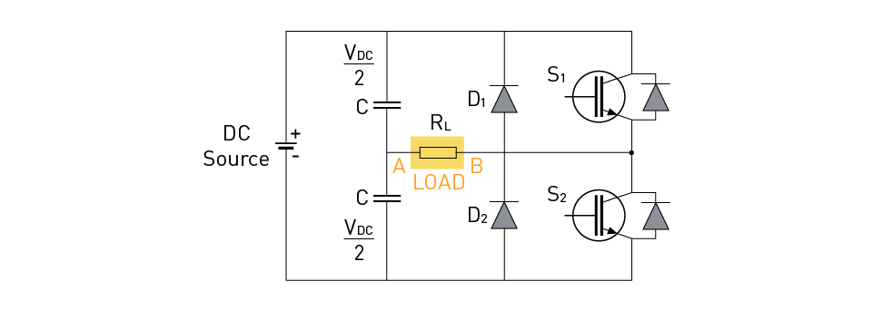
Figure 1: Typical Half H-Bridge Inverter
As depicted in Figure 1, the half-bridge inverter architecture is a basic single-phase inverter structure. It is made up of two switching components (usually transistors, IGBTs, or MOSFETs) linked in series across a DC voltage source, two feedback diodes, and two capacitors that link the source and load. The load is attached between the midpoint of the capacitors (A node) and the midpoint of the diode and switches (B node). A complementary operation of the switches creates an AC output voltage across the load in this arrangement. Feedback diodes are utilized with inductive loads. Although the half-bridge inverter is reasonably straightforward and inexpensive, it needs a center-tapped DC voltage source or a split capacitor to supply the necessary voltage.
The load in a half-bridge inverter may be resistive (R) or resistive and inductive (RL). While the current waveform for an RL load is phase-shifted to the voltage waveform, it is identical to the output waveform for a R load. The power factor of the load, which is impacted by the inductive nature of the load, determines this phase shift.
Operation with R load
The two modes of operation for a half-bridge inverter with R load are as discussed below:
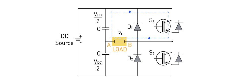
Figure 2: Mode 1 for R-Load in half H-bridge inverter
Figure 2 depicts Mode 1 for a resistive load in a half H-bridge inverter. The output voltage in this mode is equal to half the DC source voltage, current flows through the load and the top switch (S1), and the lower switch (S2) is turned off. The output voltage across the load can be measured as
$$VO = V_{dc}/2$$Similarly, the output current is measured as
$$VO / RL$$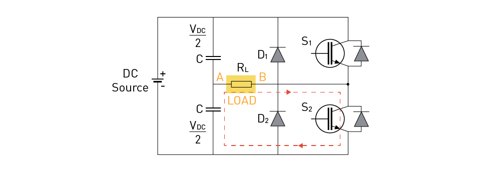
Figure 3: Mode 2 for R-Load in half H-bridge inverter
Figure 3 depicts mode 2 for resistive loads in a half-H-bridge inverter. The output voltage in this mode is equal to the negative half of the DC source voltage, current flows through the load and the lower switch (S2), and the upper switch (S1) is off.
The output voltage across the load is
$$VO = -V_{dc}/2$$Similarly, the output current is
$$VO / R_L$$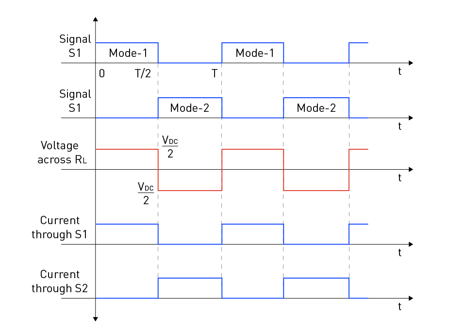
Figure 4: Waveforms of Half H-Bridge Inverter with R Load
For the half-bridge inverter with resistive load, Figure 4 depicts the waveforms of the switching signals, output voltage, and current through the switches.
It can easily be shown that the RMS value of the fundamental component of the output is equal to 0.45 Vdc.
Operation with RL load
The half-bridge inverter has four operating modes for RL load. In this type of inverter, the feedback diodes (D1 and D2) play a critical role. When the switches are off, they offer a route for the inductive load current to return to the source. This function guards against voltage spikes and guarantees a steady stream of current across the load during switching transitions.
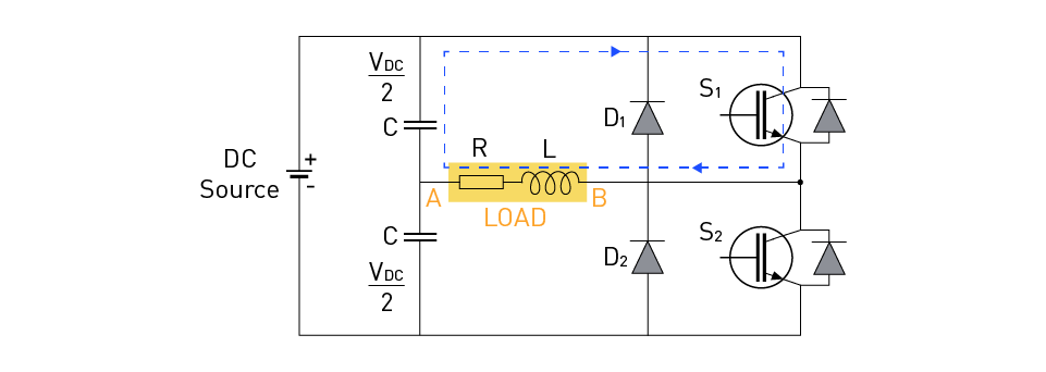
Figure 5: Mode 1 for RL-Load in half H-bridge inverter
Figure 5 depicts Mode 1 for RL load in a half H-bridge inverter. In this mode, the upper switch (S1) is turned ON and the lower switch (S2) is turned off. Here, the output voltage is equal to half the DC source voltage and current flows through the load and S1. Up until its maximum value, the current progressively climbs from zero. Due to the identical polarity of the current and voltage, the inductor will store the energy.

Figure 6: Mode 2 for RL-Load in half H-bridge inverter
Figure 6 displays Mode 2 for RL load in half H-bridge inverter. D2 switches ON in this mode and the output voltage is equal to the negative half of the DC source voltage, and current flows through the load in the same direction as in Mode-1 as the inductor resists abrupt changes in current. As the inductor discharges, the current gradually drops until the load current IL is zero.
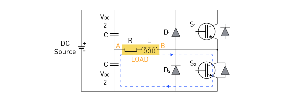
Figure 7: Mode 3 for RL-Load in half H-bridge inverter
Figure 7 displays Mode 3 for RL load in half H-bridge inverter. In this mode, the lower switch (S2) is ON after the inductor has been fully discharged through the load, and current is flowing through the load and the lower switch (S2) as the output voltage is equal to the negative half of the DC source voltage. Compared to Mode 1 and 2, the direction of the current flow through the load is reversed. Following the firing of S2, the current begins to rise and reaches a negative peak. The charge is once more stored by the inductor.
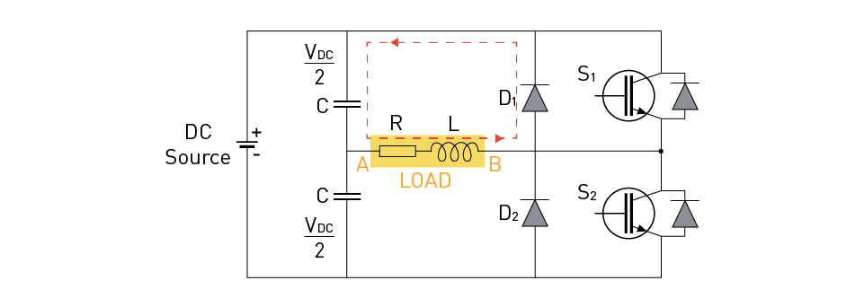
Figure 8: Mode 4 for RL-Load in Half H-Bridge Inverter
Figure 8 illustrated Mode 4 for RL load in half H-bridge inverter. When D1 is ON, the output voltage in this mode is equal to half the DC source voltage, and current flows through the load in the same direction as in Mode 3 due to the inductor's resistance to abrupt changes in current. As the inductor discharges, the current gradually drops until the load current IL is zero.
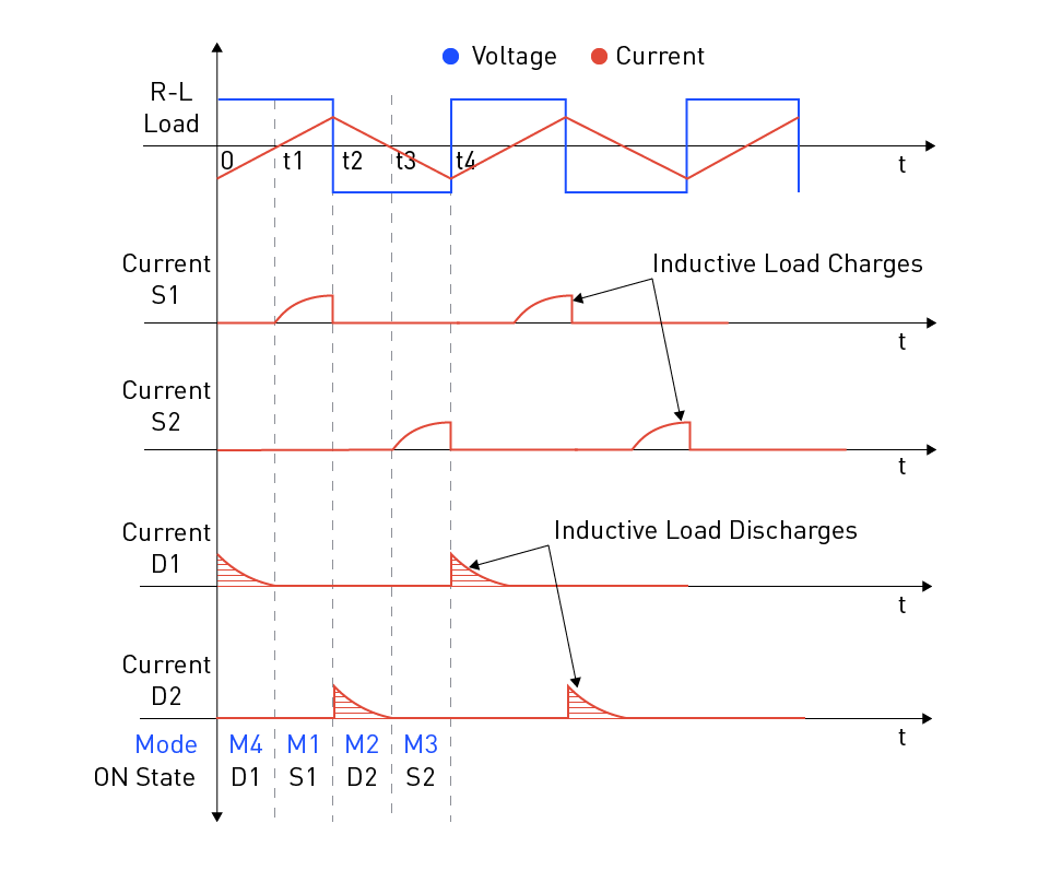
Figure 9: Waveforms of Half H-Bridge Inverter with RL Load
The waveforms of the output voltage and current as well as the current flowing through the switches and diodes for the half-bridge inverter with RL load are shown in Figure 9. The figure also depicts the on diodes and the switches along with the modes of operation M1–M4.
Full-Bridge Inverter
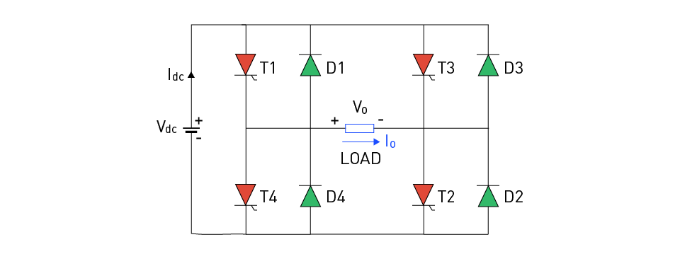
Figure 10: Full Bridge Inverter
Figure 10 illustrates the "H-bridge" arrangement of four switching devices (transistors, IGBTs, MOSFETs, or thyristors) and four feedback diodes used in a full-bridge inverter topology. In comparison to the half-bridge architecture, this topology provides a larger output voltage capability. Full-bridge inverters offer improved performance and are often used in many single-phase inverter applications, including motor drives, solar inverters, and UPS systems, despite having a larger component count and complexity.
The load in a full-bridge inverter may be resistive (R) or resistive and inductive (RL). An R load's current waveform and output voltage waveform are the same. However, due to the inductive nature of load, the current waveform for an RL load is phase-shifted to the voltage waveform. The power factor of the load affects the phase shift's magnitude.
Operation with R Load
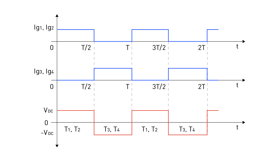
Figure 11: Full Bridge Inverter Gate Signals and Output Voltage for R Load
In Figure 11, the output voltage as well as the inverter gating signals are displayed. It may be readily shown that the fundamental component of the output has an RMS value of 0.9Vdc, which is double that of a half-bridge inverter.
For a full-bridge inverter with R load, the two primary modes of operation are:
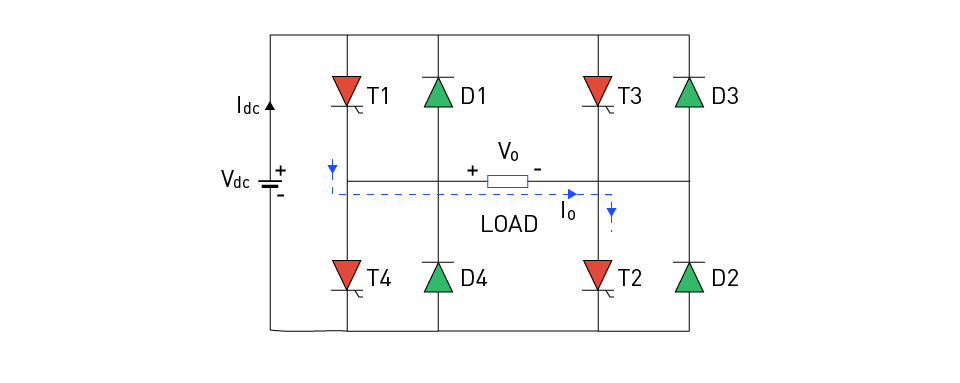
Figure 12: Mode 1 of Full Bridge Inverter with R Load
Figure 12 depicts Mode 1 for R load in a full bridge inverter. The output voltage is equal to the DC source voltage when the upper-left switch (T1) and lower-right switch (T2) are turned ON, and the upper-right switch (T3) and lower-left switch (T4) are turned OFF. Current flows through the load, the upper-left switch (T1), and the lower-right switch (T2).
Across the load, the output voltage is
$$VO = V_{dc}$$Similarly, the output current is
$$VO / RL$$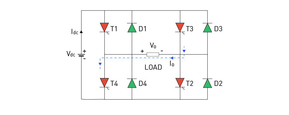
Figure 13: Mode 2 of Full Bridge Inverter with R Load
Figure 13 depicts Mode 2 for R load in a full bridge inverter. The output voltage is equal to the negative DC source voltage when the upper-right switch (T3) and the lower-left switch (T4) are turned ON and the upper-left switch (T1) and lower-right switch (T2) are turned OFF. In this case, the current flows through the load, the upper-right switch (T3), and the lower-left switch (T4).
Across the load, the output voltage is
$$VO = -V_{dc}$$Similarly, the output current is
$$VO = R_L$$Operation with RL Load
The full-bridge inverter with RL load has 4 modes of operation. The two additional modes reflect the freewheeling action. Due to the diodes' free-wheeling behavior, the polarity of the voltage across the load does not alter instantly. In applications involving RL loads, a full-bridge inverter's free-wheeling diodes (D1, D2, D3, and D4) are essential for optimal functioning. They give the inductive load current a low-impedance channel to follow while the switches shift between the ON and OFF states. The free-wheeling diodes enable the continuous flow of current through the load during the switching transitions and guard the switches from voltage spikes brought on by the inductive load, thus, improving the inverter's overall performance and reliability. The full-bridge inverter with RL load and its four modes of operation are as follows:

Figure 14: Mode 1 of Full Bridge Inverter with RL Load
Figure 14 depicts Mode 1 for RL load in a full bridge inverter. In this, switches T1 and T2 conduct transport current from source to load. Positive polarity is present across the load for the whole input voltage Vdc, and the current progressively increases until it reaches its maximum value. Due to the same polarity of the voltage and current in this mode, the inductor stores energy.
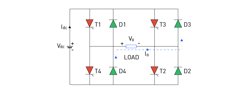
Figure 15: Mode 2 of Full Bridge Inverter with RL Load
Figure 15 depicts Mode 2 for RL load in a full bridge inverter. The feedback diodes D3 and D4 transfer the load's stored energy to the source in Mode 2. Thyristors T1 and T2 will be commutated by the feedback diodes to initiate conduction right away. Additionally, these diodes lessen the di/dt spike and negative voltage appears across the load. However, the current's polarity stays the same while steadily decreasing until it hits zero.

Figure 16: Mode 3 of Full Bridge Inverter with RL Load
Figure 16 illustrates Mode 3 for RL load in a full bridge inverter. The T3 and T4 thyristors are instantly activated in Mode 3 following the full discharge of the inductive load. The current begins to flow against it and progressively picks up speed until it reaches the negative peak. Current and voltage are both negative in Mode 3; thus, the inductor stores energy once again.
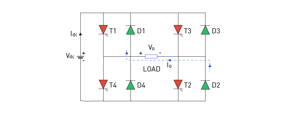
Figure 17: Mode 4 of Full Bridge Inverter with RL Load
Figure 17 depicts Mode 4 for RL load in a full bridge inverter. The feedback diodes D1 and D2 are used in Mode 4 which begin conducting as soon as the previously triggered T3 and T4 have commutated.
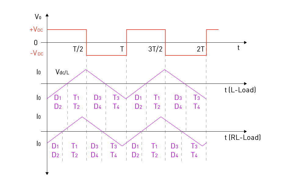
Figure 18: Output Voltage and Current of Full Bridge Inverter with L and RL Load
Figure 18 displays the output voltage and current for the complete bridge with the L and RL load. The fundamental component of current may be seen to lag behind the fundamental component of voltage. The figure shows the active diodes and thyristors for each mode.


直接登录
创建新帐号