Power Management
In the design of digital isolators with integrated power, effective power management holds paramount importance, especially concerning the optimization of system efficiency and the pursuit of sustainable energy solutions.
Techniques for Optimal Power Utilization
Dynamic Power Control: Dynamic power control implementation entails the adjustment of system power usage according to prevailing operational requirements. Techniques like dynamic voltage scaling and variable frequency operation enable the system to diminish power consumption during periods of low-load conditions.
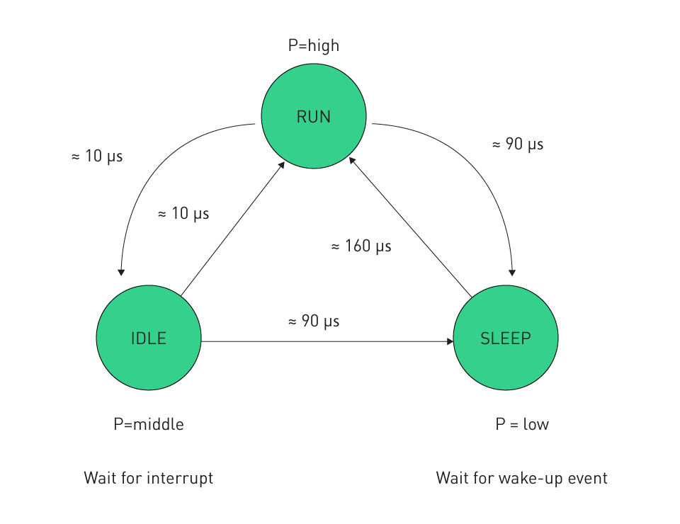
Figure 1: Example of Dynamic Power Control for an Electronic System
Low-Power Idle Modes: The integration of low-power idle modes into the design, allowing the system or specific components to enter a power-saving state during periods of inactivity, results in a significant reduction in overall power consumption.
Efficient Switching Techniques: Utilizing efficient switching techniques like synchronous rectification in systems with switching components, such as DC-DC converters, assists in minimizing switching losses, consequently enhancing power efficiency.
Advanced Semiconductor Materials: Enhanced efficiency can be achieved by utilizing semiconductors crafted from materials such as Gallium Nitride (GaN) or Silicon Carbide (SiC). Compared to traditional silicon, these materials provide higher electron mobility and faster switching capabilities, thereby resulting in reduced power losses.
Accurate Power Monitoring: The inclusion of sensors and monitoring circuits for precise power consumption measurement aids in the identification of areas for optimization and facilitates the implementation of more efficient power management strategies.
Energy Harvesting Opportunities
Solar Power: Integration of photovoltaic cells into electronic systems, particularly in portable and outdoor applications, enables the harnessing of solar energy. This proves beneficial in extending battery life or even supplying power to the system completely in low-power applications.
Thermoelectric Energy: Utilizing temperature differentials, thermoelectric generators (TEGs) have the capability to convert heat into electrical energy. This feature can be especially advantageous in industrial settings where waste heat is accessible.
Vibration and Motion Energy: Piezoelectric materials or electromagnetic transducers can be employed to convert mechanical energy into electrical energy in environments characterized by consistent movement or vibration, such as industrial machinery or vehicles.
RF Energy Harvesting: Capturing ambient radio frequency (RF) energy from sources like broadcast towers or Wi-Fi networks allows for its conversion into small amounts of electrical power, making it suitable for very low-power applications.
Integrated Energy Harvesting Solutions: The integration of several energy harvesting methods within one system can furnish a more stable and dependable power source, thereby diminishing reliance on external power supplies or batteries.
Integration and Miniaturization
Substantial advancements in system design are fueled by integration and miniaturization trends within the domain of digital isolators with integrated power. Not only do these trends mirror the evolving demands of modern electronics, but they also introduce distinct challenges and opportunities in the optimization of designs.
Achieving High-Density Integration
Compact Component Design: Incorporating high-density integration entails employing compact, multifunctional components. Within the realm of digital isolators, this translates to integrating supplementary functionalities like power management or signal processing into a singular compact package.
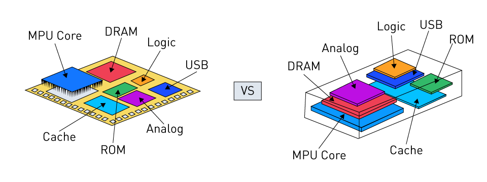
Advanced Semiconductor Technologies: By harnessing advanced semiconductor manufacturing processes, it becomes feasible to achieve smaller component sizes while preserving or enhancing performance. These techniques encompass designs such as system-in-package (SiP) or system-on-chip (SoC).
3D Packaging Techniques: 3D packaging involves vertically stacking components that can increase space utilization in electronic devices. This method proves especially advantageous in highly integrated systems such as wearable technology or smartphones.
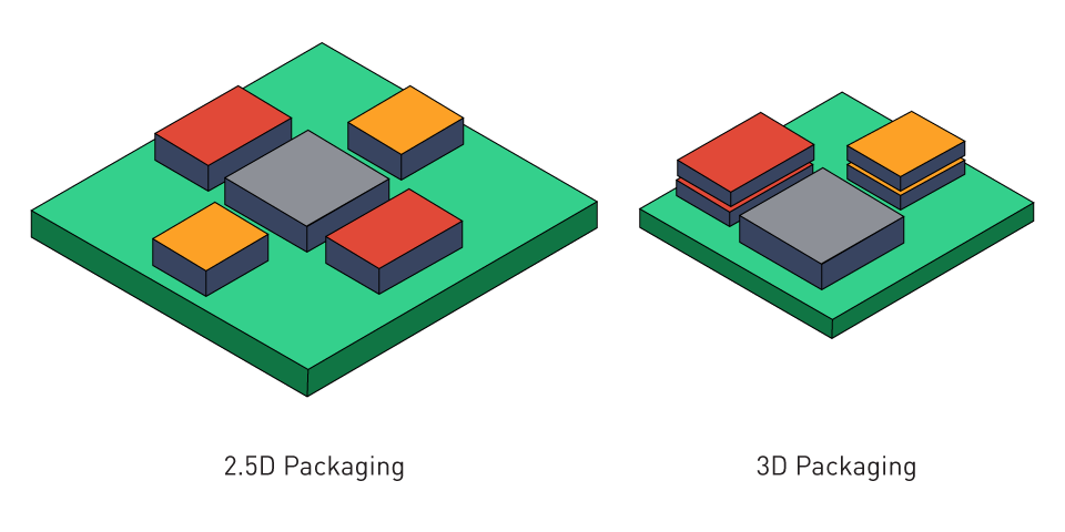
Figure 2: 3D Packaging
Optimized PCB Layout: Optimized PCB layout practices are essential for achieving high-density integration. Incorporating multilayer PCBs, micro-vias, and dense routing techniques facilitates accommodating a greater number of components within a confined area.
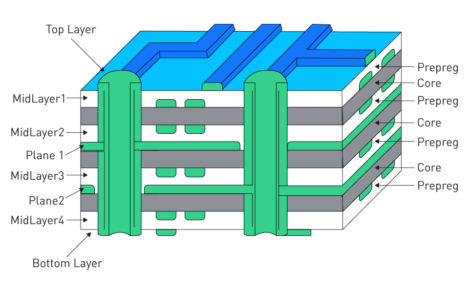
Figure 3: Multi-Layer PCB
Impact of Miniaturization on System Design
Enhanced Portability and Wearability: The development of smaller, lighter, and more portable electronic devices is facilitated by miniaturization. This holds particular significance in medical devices, consumer electronics, and wearables, where size and weight are pivotal considerations.
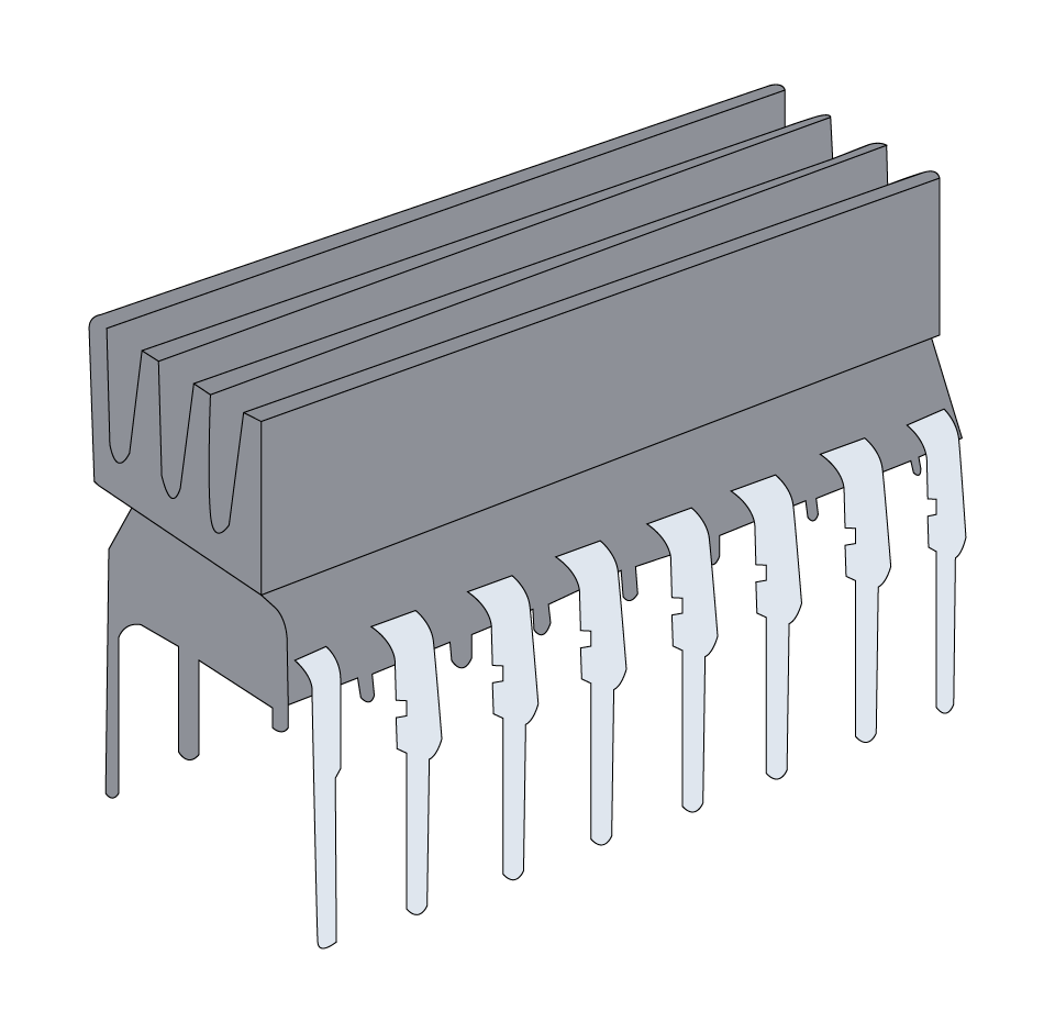
Complex Thermal Management: With denser packing of components, heat management becomes increasingly challenging. To ensure effective heat dissipation without compromising the device's size and form factor, miniaturization demands innovative thermal management solutions.
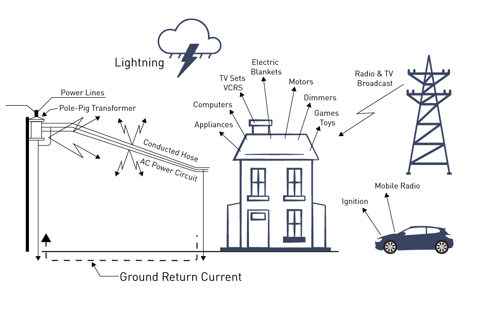
Increased Design Complexity: Increased complexity in system design often accompanies miniaturization. It is essential for designers to consider electromagnetic compatibility, intricate interconnections, and accurate assembly techniques.
Improved System Performance: The improved performance offered by miniaturized systems stems from shorter interconnects, resulting in decreased signal transmission delays and power losses. This benefit is particularly notable in computing applications and high-speed communication.
Cost Implications: Despite the potential for higher initial development costs associated with advanced manufacturing techniques and materials, miniaturization can ultimately yield cost savings through decreased material usage and enhanced functionality per unit area.


直接登录
创建新帐号