Flash ADCs
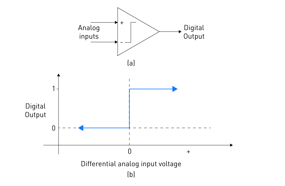
Figure 10: Comparator (a) Comparator symbol (b) Comparator input/output transfer function
Architecture
One of the most straightforward and quick types of ADC is flash ADC, commonly referred to as parallel ADC. An encoder circuit and multiple comparator circuits make up its architecture. Each comparator evaluates the analog voltage input in comparison to a reference voltage. The reference voltages are programmed to rise across the comparators in equal stages. After that, an encoder transforms the comparator outputs into a binary code that represents the digital counterpart of the analog input.
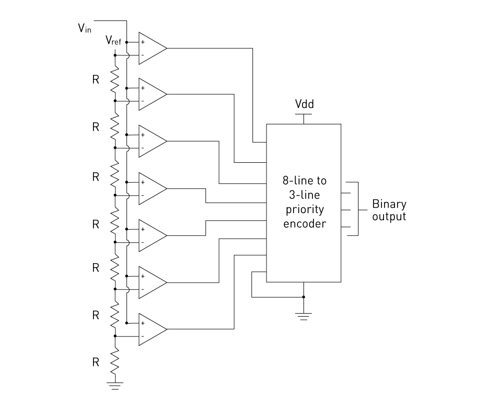
Figure 11: 3-bit flash ADC
More specifically, there are 2n - 1 comparators for an n-bit Flash ADC. Through a resistive ladder network, the stepped reference voltages are provided to the comparators. The reference voltage is divided into 2n evenly spaced steps by the resistive ladder.
Advantages and Disadvantages
Advantages:
Speed: Flash ADCs are considered as the fastest type of ADCs due to their ability of carrying out the conversion in a single step. Therefore, they are perfect for high-frequency applications.
Simplicity: A flash ADC's architecture is quite straightforward, especially for applications that require lesser resolution.
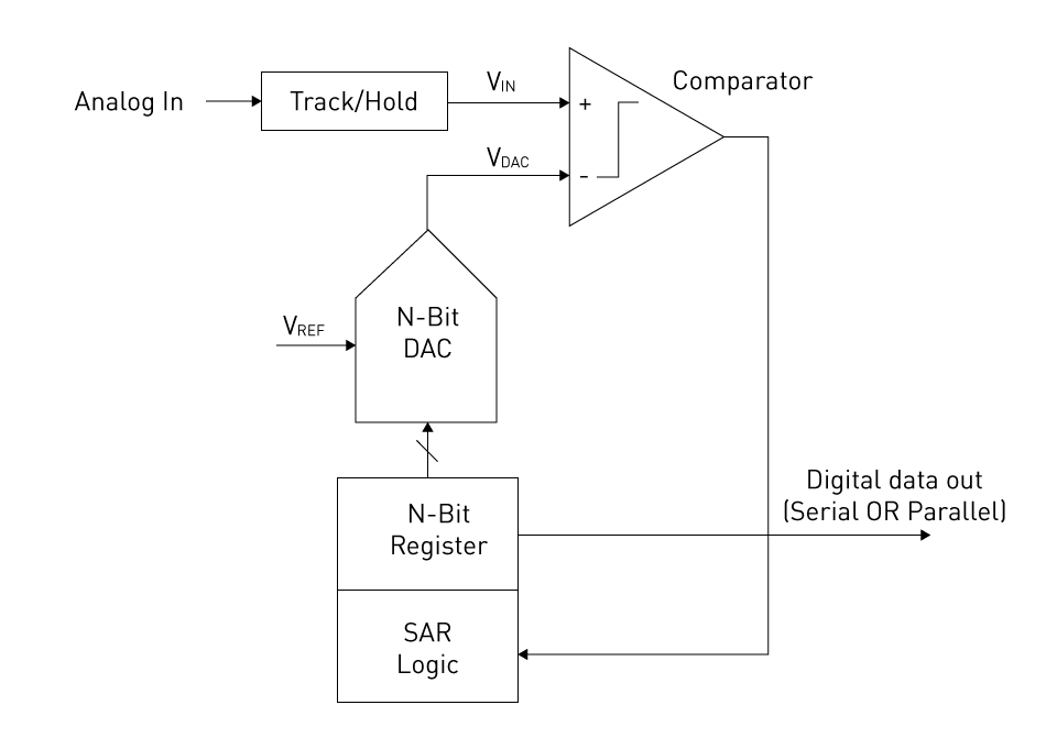
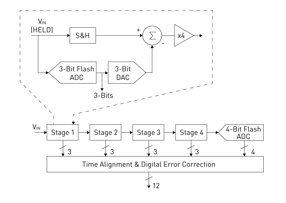
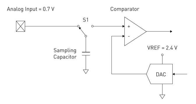
Scalability: The quantity of necessary comparators grows exponentially as the number of bits (resolution) rises. For instance, 255 comparators are needed for an 8-bit flash ADC, whereas 4095 comparators are needed for a 12-bit ADC. High-resolution applications are therefore impractical. Power Consumption and Cost: The large number of comparators results in higher expenses and increased power usage. Size: Flash ADCs can be substantial due to the huge number of components, especially for high resolution applications. Speed-sensitive applications frequently employ Flash ADCs. Applications that are often used include: Digital Oscilloscopes: utilized to capture high-speed signals High-Frequency Signal Acquisition: For instance, radar systems where real-time data processing is required. Video and Image Processing: When parallel conversion of large amounts of data is required. Communication Systems: Particularly when superheterodyne receivers convert IF (Intermediate Frequency) signals to digital format. Figure 12: Simplified SAR ADC architecture SAR stands for Successive Approximation Register. The common ADC type known as ADC strikes a good compromise between conversion speed and complexity. A sample and hold circuit, a comparator, a successive approximation register, and a DAC (Digital to Analog Converter) make up its four main structural elements. The sample and hold circuit captures the input analog voltage at the beginning of the conversion process and retains it throughout. A binary search is then started by the successive approximation register to locate the digital equivalent of this analog voltage. First of all, the register sets the most significant bit (MSB) to 1 and the rest to 0, and the value is passed to the DAC, which turns it into an analog voltage. The comparator compares this voltage to the input voltage. The bit remains set if the DAC output is smaller than the input voltage; otherwise, it is cleared. Up until the least significant bit (LSB), the process is repeated bit by bit to provide the closest possible digital copy of the analog input. Good Trade-off Between Speed and Complexity: SAR ADCs are slower than flash ADCs, but faster than some ADCs, such as integrating ADCs. They are more practical for medium to high resolutions since they require fewer components than flash ADCs. Lower Power Consumption: SAR ADCs use less power than flash ADCs, especially at slower sampling rates. Compact Size: SAR ADCs typically have fewer components than flash ADCs with the same resolution, making them physically smaller. Compact Size: SAR ADCs typically have fewer components than flash ADCs with the same resolution, making them physically smaller. Not Suitable for Very High Speeds: Since the successive approximation procedure requires several clock cycles, it is not appropriate for really fast applications. Variable Conversion Time: Timing in some systems can become more challenging because the conversion time may slightly vary depending on the input. Data Acquisition Systems: This includes sensor interfacing, which calls for modest speed and resolution. Microcontrollers: SAR ADCs are commonly integrated into microcontrollers for general-purpose analog to digital conversion. Audio Processing: Utilised when high resolution is needed but not ultra-high rates for sound recording and processing. Instrumentation: Utilised in digital multimeters and various measurement devices. Battery-Powered Devices: Due to their low power requirements, SAR ADCs are perfect for battery-powered applications. A variant kind of analog-to-digital conversion is used by Delta-Sigma (ΔΣ) or Sigma-Delta (ΣΔ) ADCs, which additionally include oversampling, noise shaping, and digital filtering methods. A decimation filter and a delta-sigma modulator make up the majority of the design. A crucial component is the Delta-Sigma modulator, which combines an integrator (sigma) with a difference operation (delta). The modulator works by rapidly oversampling the input signal, usually at a rate substantially higher than the Nyquist rate. The quantization noise is pushed to higher frequencies by noise shaping, which comes after oversampling. By eliminating the high-frequency quantization noise, the decimation filter also lowers the data rate to a more tolerable level. The resolution and dynamic range of the ADC are efficiently increased by combining oversampling with noise shaping. High Resolution and Accuracy: The quantization noise is successfully dispersed over a wide range using the noise shaping approach, greatly lowering the noise floor. Due to this, Delta-Sigma ADCs may attain high resolutions, making them perfect for applications requiring accuracy. Effective for Low-Frequency Applications: Since Delta-Sigma ADCs have a construction that greatly reduces noise at lower frequencies, they are excellent for low-frequency or DC measurements. Increased Complexity: The approaches for noise shaping and oversampling make Delta-Sigma ADCs more sophisticated. Costs may increase as a result of this complexity, particularly for higher-order modulators. Latency: In some applications that need real-time response, the oversampling procedure and decimation filter impose a delay that might be troublesome. Not Suitable for High-Speed Applications: The oversampling approach can enhance resolution but is not appropriate for high-speed signal processing. Precision Measurement Devices: These include weighing scales, digital multimeters, and other devices that call for extremely precise measurements. Audio Applications: Due to its excellent resolution and low noise properties, Delta-Sigma ADCs are often used in both professional and consumer audio applications. Industrial Process Control: Delta-Sigma ADCs are employed in a variety of industrial operations where low-frequency measurement and high precision are essential. Seismic and Environmental Monitoring Systems: Delta-Sigma ADCs are ideally suited for monitoring minute fluctuations in environmental and seismic activity because of their excellent resolution. Figure 13: 12-bit pipelined ADC To convert an analog input to a digital output, pipeline analog-to-digital converters (ADCs) employ a cascaded structure with a number of stages. In the pipeline, each step is in charge of transforming a portion of the incoming signal and sending the leftover to the following stage. A pipeline ADC's fundamental design often consists of several stages, with each stage containing an inter-stage gain amplifier, a DAC, a lower-resolution ADC (commonly a flash ADC), and a sample-and-hold circuit. Afterwards, a digital error correcting block comes as the last stage. The first stage samples the analog input during operation and then transforms a portion of the signal to digital. The analog signal is then recreated using the stage's converted digital output, which is subsequently subtracted from the sample's original value to leave a residue. The procedure is repeated at the following stage once this residue has been amplified. The ultimate high-resolution digital output is created by combining all of the digital outputs from the pipeline's stages and correcting them for flaws. High-Speed Conversion: Pipeline ADCs may achieve high-speed conversion rates because of the parallel processing in the pipeline stages, making them appropriate for applications needing medium to high resolutions at rapid speeds. Good Trade-off Between Speed and Resolution: A balanced trade-off between conversion speed and resolution is provided by pipeline ADCs, which is advantageous for many applications. Latency: Pipeline ADCs have inherent delay since the conversion procedure is multi-stage. Before a conversion can be said to be finished, a sample must go through each stage. Complexity and Power Consumption: In comparison to other ADC architectures like SAR ADCs, the multi-stage architecture is more sophisticated and uses more power. Telecommunications: In order to convert intermediate frequency (IF) signals to digital format, pipeline ADCs are frequently utilized in telecommunication systems. Digital Imaging: When a high-speed, medium-to-high resolution conversion is needed, it is used in image sensors and scanners. High-Speed Data Acquisition Systems: Used in applications like oscilloscopes where data must be gathered quickly without sacrificing resolution too much. Software-Defined Radios: Pipeline ADCs are a crucial component of Software-Defined Radios when broad bandwidth digitizing is needed. Figure 14: Dual-slope integrating ADC Dual-slope ADCs, sometimes referred to as integrating ADCs, use an integrator to average the input voltage across a predetermined time interval. An integrator, a reference voltage source, a comparator, and a digital counter generally make up the architecture. A known reference voltage is applied in the opposite polarity until the integrator output reaches zero after the input voltage has been integrated for a certain amount of time. In proportion to the input voltage, the counter measures the number of clock cycles required to achieve zero. Advantages: Noise Reduction: Integrating ADCs significantly minimize noise and interference by averaging the input across time. High Accuracy: Due to its innate linearity, it is appropriate for precise measurements. Disadvantages: Slow Conversion Speeds: Due to its inherent sluggishness, dual-slope integration is inappropriate for high-speed applications. Complexity: Compared to other ADC kinds, the design may be more complex due to the requirement for precision components. Digital Multimeters: Used when speed is not a factor in high-precision voltage measurements. Weigh Scales: Used for precise weight readings in electronic weigh scales. Figure 15: Time-interleaved ADC Time-Interleaved ADCs use many ADCs running simultaneously, with each ADC sampling at a little bit of a separate time. With this design, the sampling rate is effectively increased by a factor that is proportional to the number of ADCs. A high-speed, high-resolution digital output is produced by combining the outputs from the parallel ADCs. Advantages: High-Speed Conversion: Time-interleaved ADCs can reach exceptionally high sampling rates by employing several ADCs simultaneously. Increased Effective Resolution: For some applications, the parallel design can also improve the effective resolution. Disadvantages: Calibration Challenges: Errors might result from mismatches between the parallel ADCs, and calibration can be difficult. Increased Complexity and Power Consumption: Combining ADCs increases circuit complexity and energy usage. High-Speed Communications: Used when incredibly high data rates are required for high-speed communication networks. Radar Systems: Used in radar systems to process signals quickly. Medical Imaging: Used in medical imaging systems when quick, high-quality data capture is essential.
Table 1: ADC comparison matrix The precise needs of a given application, such as conversion speed, resolution, complexity, and power consumption, are what ultimately dictate the choice of an ADC design. We will compare different ADC kinds, such as Flash, SAR, Delta-Sigma, Pipeline, Integrating, and Time-Interleaved ADCs, depending on these properties. Flash ADCs: Provides the quickest conversion speeds, which qualifies them for applications requiring extremely quick data conversion. Time-Interleaved ADCs: ADCs can be used in parallel to achieve high conversion speeds, however they are slower than Flash ADCs. Pipeline ADCs: Demonstrate fast conversion rates, but with some latency brought on by the pipeline phases. SAR ADCs: They are appropriate for applications that do not demand ultra-high-speed conversion and have modest conversion speeds. Delta-Sigma ADCs: Due to oversampling and filtering, this type of processing is typically slower. Integrating ADCs: Due to their functioning on two slopes, this type is the slowest. Delta-Sigma ADCs: The excellent resolution of delta-sigma ADCs makes them perfect for high-precision measuring applications. Integrating ADCs: By averaging the input across time, great resolution is provided. SAR ADCs: These are adaptable for a variety of applications and provide good resolution. Pipeline ADCs: Depending on the design, they offer moderate to high resolution. Time-Interleaved ADCs: Resolution can be efficiently increased, however calibration issues could occur. Flash ADCs: Due to a lot of comparators needed for high resolution, flash ADCs often have lesser resolution. Flash ADCs: High complexity from numerous comparators; more power usage. Time-Interleaved ADCs: As there are more parallel ADCs, complexity and power usage rise. Pipeline ADCs: Moderate complexity; scaling of power consumption with stage count. Delta-Sigma ADCs: Due to filtering and decimation, Delta-Sigma ADCs are moderately complex; power consumption varies. SAR ADCs: Low power consumption and relatively simple construction. Integrating ADCs: Low power consumption; relatively simple, however precision components might add complexity. Flash ADCs: The ADC architecture that uses the large number of comparators per conceivable output value is typically the largest. More comparators are required for greater bit resolutions, which increases size. Time-Interleaved ADCs: With several ADCs operating in parallel, the size can also be fairly enormous. The increase in size may, however, be smaller than an equivalent increase in the bit resolution of a flash ADC because each individual ADC may be of a simpler form. Pipeline ADCs: As the circuitry is broken down into various stages, each of which contributes to a distinct aspect of the overall conversion process, pipeline ADCs often have moderate sizes. However, a larger total size may result from adding more pipeline stages in order to achieve higher resolution or faster performance. Delta-Sigma ADCs: These ADCs use oversampling and filtering techniques, therefore their size is moderate. The use of large oversampling ratios and multi-bit quantizers might make the circuit larger when a digital filter is included. SAR ADCs: SAR ADCs typically have smaller architectures than other types since they operate with fewer components and have a simpler design. To accommodate a more accurate DAC and comparator, the size of the SAR ADC can also grow as the bit resolution does, though. Integrating ADCs: The smaller sizes of these ADCs are a result of their simpler construction. The integrator, comparator, and a counter make up the primary parts. The size might, however, somewhat rise if the integrator needs high-precision resistors and capacitors. Table 2: ADC size comparison Flash ADCs: Oscilloscopes and high-frequency systems use flash ADCs. SAR ADCs: Flexible, utilized in data acquisition systems and microcontrollers. Delta-Sigma ADCs: Precision measurements and audio processing. Pipeline ADCs: For wireless communication and video processing. Integrating ADCs: Precision measurements in digital multimeters and weigh scales. Time-Interleaved ADCs: Radar systems and high-speed communications.Disadvantages:
Typical Applications
SAR ADCs
Architecture
Advantages and Disadvantages
Advantages:
Disadvantages:
Typical Applications
Delta-Sigma ADCs
Architecture
Advantages and Disadvantages
Advantages:
Disadvantages:
Typical Applications
Pipeline ADCs
Architecture
Advantages and Disadvantages
Advantages:
Disadvantages:
Typical Applications
Other ADC Architectures - Integrating ADCs
Architecture

Advantages and Disadvantages
Typical Applications
Other ADC Architectures - Time-Interleaved ADCs
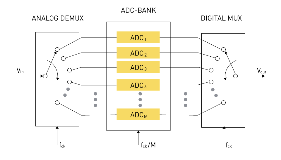
Architecture
Advantages and Disadvantages
Typical Applications
Comparative Analysis Of ADC Types
FLASH (Parallel)
SAR
DUAL SLOPE (Integrating ADC)
PIPELINE
SIGMA DELTA
Pick this architect if you want:
Ultra-High Speed when power consumption not primary concern.
Medium to high resolution (8 to 20 bits), 5 Msps and under, small size, low power.
Monitoring DC signals, good noise performance ICL7106, low power consumption, high resolution.
Lower power consumption than flash, High speeds, few Msps to 100+ Msps, 8 bits to 16 bits.
Low to medium speed, no precision external components, high resolution, simultaneous 50Hz/60Hz rejection, digital filter reduces anti-aliasing requirements.
Conversion Method
N bits - 2N-1 Comparators, Caps rises by a factor of 2 for each bit.
Binary search algorithm, internal circuitry runs higher speed.
Unknown input voltage is integrated and value compared against known reference value.
Small parallel structure, each stage works on one to a few bits.
Oversampling ADC, 5Hz to 60Hz rejection programmable data output.
Encoding Method
Thermometer Code Encoding
Successive Approximation
Analog Integration
Digital Correction Logic
Oversampling Modulator, Digital Decimation Filter
Disadvantages
Sparkle codes/metastability, high power consumption, expensive, large size.
Speed limited to 5Msps, may require anti-aliasing filter.
Slow conversion rate, high precision external components required to achieve accuracy.
Parallelism increases throughput at the expense of power and latency.
Higher order (4th order on higher) - multibit ADC and multibit feedback DAC.
Conversion Time
Conversion time does not change with increased resolution.
Increases linearly with increased resolution.
Conversion time doubles with every bit increase in resolution.
Increases linearly with increased resolution.
Tradeoff between data output rate and noise free resolution.
Resolution
Component matching typically limits resolution to 8 bits.
Component matching requirements double with every bit increase in resolution.
Component matching does not increase with rise in resolution.
Component matching requirements double with every bit increase in resolution.
Component matching requirements double with every bit increase in resolution.
Size
2N-1 Comparators, Die size and power grows exponentially with rise in resolution.
Die grows linearly with rise in resolution.
Core die size won't significantly change as resolution rises
Die grows linearly with rise in resolution.
Core die size won't significantly change as resolution rises
Conversion Speed
Resolution
Complexity and Power Consumption
Size and Component Count
Flash
Die size and power rises exponentially as resolution increases
Pipeline
Die size rises linearly with resolution
Sigma-Delta
Core die size won't significantly change as resolution rises
Successive Approximation (SAR)
As resolution increases, there won't be much of a difference in core die size
Time-interleaved
Die size grows semi-exponentially as resolution improves
Integrating ADCs
Smaller die sizes result from simple architecture
Typical Applications




直接登录
创建新帐号