Introduction to Integrating ADCs
The basic function of an Analog-to-Digital Converter (ADC) is to transform a continuously fluctuating analog signal into a discrete or binary digital signal. The need for a wide range of ADCs with varying performance characteristics has resulted in the development of numerous architectures, one of which is the Integrating ADC.
The Integrating ADC, sometimes called a charging or ramp ADC, is a kind of ADC that changes signals by timing how long it takes for an integrator to go up and down. The word "integrating" means adding up the input signal. It adds or combines the input signal over a set time to make a value that matches the input. Then, this added-up value is turned into a digital version.
An important feature of Integrating ADCs is their built-in capability to smooth out or combine the signal over time. This helps in getting rid of unwanted noise or filtering. This quality makes them suitable for applications where having a good balance between signal strength and noise is very important, like in precise measurement and instrumentation with high precision.
In the upcoming sections, we'll explore more about the structure of Integrating ADCs. We'll look at how they work, their pros and cons, and where they are commonly used. We'll begin by talking about the three main types of Integrating ADCs: Single Slope, Dual Slope, and Multi-slope ADCs.
Architecture of Integrating ADCs
Single Slope ADC

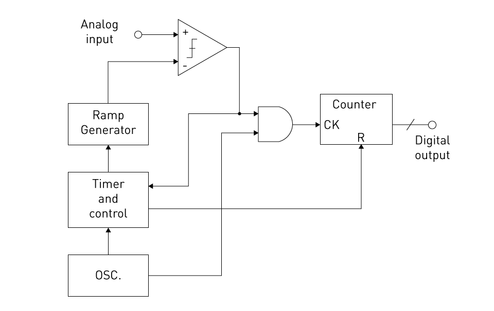
Figure 7: Single slope ADC
The single slope ADC is the most basic type of integrating ADC. It operates on a very simple concept. An integrator, a comparator, and a digital counter are part of the architecture. The integrator's output increases linearly with time since the input voltage is integrated over a given time interval. Following the integration phase, the counter is activated, and the integrator begins to discharge at a constant rate until it reaches zero. At this time, the value of the counter matches the magnitude of the input voltage. Although basic, this ADC type is somewhat sluggish because it relies on a single ramp or slope for conversion.
Dual Slope ADC

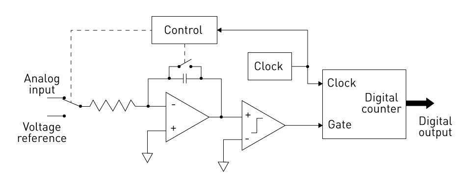
Figure 8: Dual slope ADC
The dual-slope ADC is an enhancement over the single-slope ADC in terms of precision and noise immunity. However, the architecture is slightly more complicated as it has two distinct conversion phases: run-up and run-down. The input voltage is integrated for a defined period during the run-up phase and the integrator output rises. During the run-down phase, an opposite-polarity known reference voltage is applied, and the integrator output begins to decrease. The amount of time it takes for the integrator output to return to zero is measured and used to calculate the input voltage. Dual slope ADCs reduce mistakes caused by the comparator and integrator offset voltages substantially.
Multi-Slope ADC
The multi-slope ADC is a modification that increases speed without losing precision. This ADC operates similarly to the dual-slope ADC, except during the run-down phase, multiple slopes or ramp rates are introduced. The different ramp rates enable a coarse and fine adjustment phase, resulting in faster conversion times. The coarse adjustment utilizes a faster ramp rate for a faster approach to zero, while the fine adjustment employs a slower rate for a more precise measurement. As a result, multi-slope ADCs provide more resolution and precision while delivering faster conversion times than single and dual-slope ADCs.
Operation of Integrating Dual-Slope ADCs
The functioning of an Integrating Dual-Slope ADC is divided into two stages: run-up and run-down. Each phase is essential to the ADC's operation and has an impact on its accuracy and resolution.

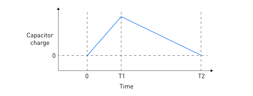
Figure 9: Run-up and run-down phases
Run-up phase: This stage begins when the input signal is introduced to the integrator for a set duration, usually controlled by a precise timer. The integrator's output grows steadily as time passes, forming a ramp that corresponds to the size of the input signal. Essentially, this step is about adding up the input signal over the designated time frame, much like an integration process.
Run-down phase: After the run-up phase is finished, an opposite-polarity reference voltage is applied to the integrator. As a result, the integrator's output starts decreasing linearly, aiming to reach zero. During this phase, a counter which keeps track of the time is employed. The count stops when the integrator output crosses the zero level, detected by a zero-crossing detector. The time measured by the counter during this phase directly represents the input voltage.
The beauty of the conversion process lies in its ability to reject common-mode noise and offsets through the dual-slope technique. The precise timing measurement during the run-down phase leads to high resolution, which makes Dual-Slope ADCs appealing for tasks needing high precision, like digital multimeters and precise measurement instruments.
Advantages of Integrating ADCs
Integrating ADCs, particularly dual-slope ADCs, brings several advantages to the table, enhancing their utility in a variety of precision measurement applications.
High Resolution: One of the most significant benefits of incorporating ADCs is their innate high resolution. The conversion technique is based on measuring time with exceptional precision, allowing for accurate and fine-grained measurements. This high resolution is especially useful in applications where minute changes in the input signal must be precisely caught.
Noise and Interference Rejection: Integrating ADCs excel at noise rejection, especially when the noise frequencies align with integer multiples of the inverse of the integration time. This effective noise reduction stems from the dual-slope technique, where noise is smoothed out during integration, notably decreasing its impact on measurements.
High Linearity: The linearity of integrating ADCs is exceptional because the conversion comprises a linear ramp and time measurement, both of which can be precisely controlled. Because of the ADC's great linearity, the output is directly proportional to the input, which is a highly desirable quality in many applications.
In summary, integrating ADCs offer a strong solution for tasks requiring high precision and low speed. They excel in maintaining linearity, resolution, and noise rejection, which are crucial factors. Recognizing their operation and applications is vital to fully harness their usefulness.
Disadvantages of Integrating ADCs
While integrating ADCs come with many benefits, it's crucial to also recognize their limitations. This awareness helps in making well-informed choices when deciding whether to employ them in different applications.
Low Conversion Rate
A significant drawback of integrating ADCs is their relatively slow conversion speed. This is a result of their operation, involving integration followed by de-integration. This sequential process inherently restricts the speed of conversion. Although longer integration times can deliver high resolution and exceptional noise rejection, it comes at the expense of conversion speed. This makes ADC integration unsuitable for high-speed conversion applications.
The sluggish conversion speed might hinder the use of integrating ADCs in high-speed scenarios or those needing real-time data processing. Thus, when picking an ADC architecture for a specific application, it's important to consider the required resolution and conversion speed to ensure the chosen ADC aligns with all necessary performance requirements.
While integrating ADCs has a low conversion rate, their high resolution, noise rejection, and linearity frequently make them an attractive choice for low-frequency, high-accuracy applications where speed is less crucial. Understanding these trade-offs can thus lead to more accurate and efficient design decisions.
Applications of Integrating ADCs
The distinct characteristics of integrating ADCs: high resolution, robust noise, interference rejection, and high linearity makes them an appealing alternative for certain applications requiring these capabilities.
Digital Multimeters and Measuring Instruments
Digital multimeters (DMMs), are flexible devices used to measure voltage, current, and resistance. They are one of the most common applications for integrating ADCs. Integrating ADCs' high resolution and precision are vital for DMMs, where correct readings are critical.
Dual-slope ADCs are commonly employed in Digital Multimeters (DMMs) due to their effectiveness. This method offers a straightforward yet efficient means of converting voltage into digital data. Its built-in ability to disregard noise spikes during measurements makes it well-suited for DMMs, enhancing accuracy.
Integrating ADCs find extensive use in other precision measuring tools like impedance analyzers and LCR meters, which assess inductance (L), capacitance (C), and resistance (R). These instruments demand the exceptional linearity and high-resolution capabilities provided by integrating ADCs.
These examples highlight how integrating ADCs are well-matched for tasks requiring precise and reliable measurements. Despite not being the fastest in conversion, their precision, noise rejection, and linearity make them a suitable choice for devices like DMMs and measurement tools. This underscores the idea that selecting an ADC architecture greatly depends on the specific needs of the application.
Design Considerations and Trade-Offs
When creating a system that includes an integrating ADC, various factors and compromises must be taken into account.
The foremost consideration is aligning with the application's unique demands. For instance, if precision and resistance to noise hold more significance than rapid conversion, opting for an integrating ADC might be the best decision, even if it tends to have a slower conversion rate. This is particularly true for devices like digital multimeters and precision measuring instruments.
The physical characteristics of integrating ADCs, including power usage and size, are extremely significant. When designing a system, it's crucial to ensure that the chosen ADC aligns with power constraints and physical size limits. These considerations are particularly vital for portable devices running on batteries.
The nature of the input signal should also be taken into account. If the input signal changes slowly or is mostly constant (DC), the relatively slower conversion speed of integrating ADCs is not a drawback. However, when dealing with rapidly changing input signals, the slower conversion rate of integrating ADCs becomes a notable limitation. In such cases, other ADC architectures like successive approximation or flash ADCs might be more appropriate choices.
Another consideration is the expected ambient conditions. Integrating ADCs are relatively resistant to temperature variations, which makes them suitable for applications where high environmental stress is anticipated.
In terms of cost, integrating ADCs are generally affordable and thus a good choice for cost-sensitive applications. However, it's important to evaluate whether their slower conversion rates and potentially higher power consumption present a trade-off that might justify the higher cost of other ADC types for your specific application.


直接登录
创建新帐号