Introduction to ADC errors
Analog-to-digital converters (ADCs) are essential for converting analog signals into digital data that can be processed by digital systems. The effectiveness of subsequent digital signal processing depends critically on the precision of this conversion, which also affects the standard of the digital representation.
Importance of Accuracy
The precision of Analog-to-Digital Converters (ADCs) holds immense significance, as it establishes the proximity of the digital output from an ADC to the actual value of the input analog signal. This holds immense weight in domains like healthcare apparatus, exacting measuring equipment, and audio manipulation. Even a minor discrepancy in the conversion process can carry substantial repercussions. To illustrate, in medical imaging, an inaccuracy might trigger an incorrect assessment of a patient's condition. Similarly, when dealing with audio manipulation, it has the potential to induce distortion or compromise the overall sound quality. Hence, a comprehensive grasp of error factors within ADCs and their mitigation becomes pivotal in upholding the credibility of the transformed data.
Effect of Errors on ADC Performance
ADCs encounter various origins of inaccuracies and errors, this include offset errors, gain errors, linearity errors, quantization errors, noise, and jitter. Each of these factors exerts distinctive influences on the performance of the ADC:
Offset Errors: Offset error manifests as a consistent disparity between the genuine output of the ADC and the theoretical output. Consequently, the entire transfer function experiences a displacement. In scenarios necessitating precise direct current (DC) precision, like the acquisition of sensor data, offset errors possess the potential to yield substantial deviations from the authentic values.
Gain Errors: Gain error corresponds to a divergence in the gradient of the ADC's transfer function from the ideal gradient. This discrepancy might lead to an amplified or attenuated representation of the input signal. The significance of gain errors is more pronounced in applications such as spectroscopy, wherein meticulous amplitude information holds crucial importance.
Linearity Errors: Errors related to linearity, encompassing Differential Non-Linearity (DNL) and Integral Non-Linearity (INL), relate to deviations in the transfer characteristics of the ADC from a straight line. This departure impacts the consistency of quantization levels, which is notably adverse in applications demanding remarkable precision.
Quantization Errors: Quantization errors denote the distinction between the actual analog input and the nearest digital representation. Inherent to the process of analog-to-digital conversion, this phenomenon impacts the ADC's resolution.
Noise: Various forms of noise, encompassing thermal noise and quantization noise, introduce stochastic fluctuations into the signal. This interference can impede the ADC's capacity to distinguish minor signal variations, posing significant challenges, particularly within applications involving low-amplitude signals.
Jitter: Jitter refers to fluctuations in the timing of the sampling clock. Its primary impact is on high-frequency signals, introducing uncertainty in the temporal domain. Consequently, this uncertainty can translate into errors in the magnitude of the digitized signal.
Offset Errors
In Analog-to-Digital Converters (ADCs), discrepancies stemming from offset errors stand as foundational origins of inaccuracies that can undermine the fidelity of digital renderings of analog signals. Acquiring comprehensive knowledge regarding offset errors, discerning their repercussions, and grasping techniques to gauge and alleviate them becomes pivotal in ADC design and application.
Definition
When the input is at zero scales or the minimum, offset error is the difference between the ADC's output and the ideal output. The output values shift across the full input range as a result of the addition of a constant bias to every conversion. The offset mistake creates a change in the code transition points by moving the transfer function along the horizontal axis.
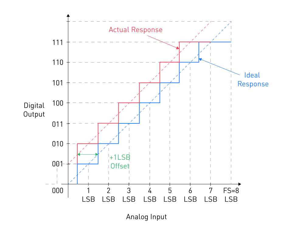
Figure 1: A graph showing the +1 LSB offset, the actual response, and the ideal response
In a unipolar three-bit ideal ADC, the initial transition should take place at 0.5 Least Significant Bit (LSB), leading to a shift in the output from 000 to 001. However, examining the actual response, as depicted in Figure 1 reveals that the ADC output changes from 001 to 010 at the 0.5 LSB mark. In the ideal scenario, the transition from 001 to 010 should occur at 1.5 LSB. Consequently, this signifies that the non-ideal response is shifted by 1 LSB towards the left in comparison to the ideal characteristic. This discrepancy is defined as a +1 LSB offset error. By considering the linear model of the non-ideal response (illustrated as the orange line in the figure), it becomes apparent that the system yields an output of 001 for a 0V input, signifying a +1 LSB offset.
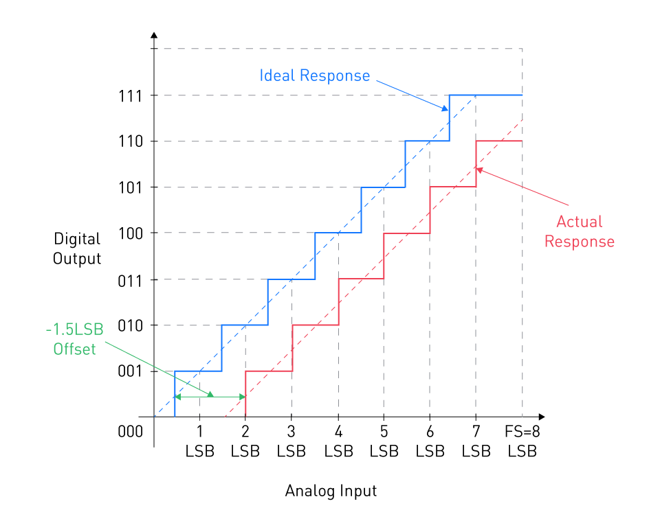
Figure 2: Response of an ADC with -1.5 LSB offset error
Causes
The primary causes of offset errors include:
Component Mismatches: Flaws and irregularities arising during the fabrication of internal ADC elements, like resistors and capacitors, can induce discrepancies that manifest as offset errors.
Temperature Drift: Shifts in ambient temperature have the capacity to modify the attributes of electronic components, provoking alterations in their values, and thereby yielding offset errors.
Supply Voltage Variations: Oscillations in the supply voltage have the potential to impact the reference voltage and the scope of analog input, ultimately leading to offset errors.
Impact on ADC Output
The ADC output values move uniformly when there is an offset error. This may be seen as shifting the ADC's entire transfer characteristic upwards or downwards. The implication is that the ADC output will show a non-zero number even when the input is zero or at its minimum. In applications that call for precise DC measurements or in differential measurement systems where small voltage variations are crucial, this can be particularly challenging.
Methods for Measuring Offset Error
Characterizing and correcting this problem in an ADC requires measuring the offset error. These are the typical approaches:Direct Measurement: Initiate the ADC with the minimum input (commonly zero voltage) and record the resultant digital output. The disparity between this reading and the ideal output (typically zero) signifies the offset error.
Best Fit Line Method: Employ an array of recognized input voltages for the ADC and construct a graph of the corresponding output values. By fitting a line through these points using a linear regression algorithm, the divergence of this line from the anticipated zero input-output characterizes the offset error.
Histogram Method: Implement a known constant voltage in proximity to the midpoint of the ADC's input range and gather a substantial quantity of samples. Crafting a histogram from this dataset unveils the mean value. Comparing this mean value with the input value facilitates the revelation of the offset error.
It is crucial to remember that if the offset error is calculated, it is frequently possible to adjust and compensate for it in software by adding a correction factor to the ADC's output during the processing phase.
Gain Errors
Gain error is a significant source of mistakes in Analog-to-Digital Converters (ADCs). For ADC systems to function accurately and dependably, it is essential to comprehend their definition, causes, and effects as well as the measuring techniques.
Definition
Gain error, also known as full-scale error, is the difference between the actual and ideal output slopes of an ADC. It denotes a scaling mistake, where the output of the ADC is either compressed or stretched relative to the ideal linear response, to put it simply. The gain mistake is depicted in Figure 3 for clarity.
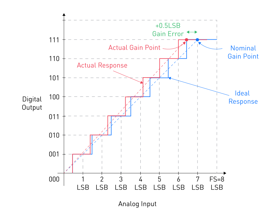
Figure 3: A graph showing the concept of gain error
Let us establish the term "gain point" as being half an LSB above the previous transition. Once the offset error is rectified, the discrepancy between the anticipated gain point and the realized gain point ascertains the gain error.
Within the aforementioned instance, the non-ideal characteristic demonstrates a gain error of +0.5 LSB. The orange line within the figure stands as the linear representation of the non-ideal response. It's apparent that a variance between the measured gain point and the theoretical gain point indeed modifies the gradient of the system's linear model. Displayed in Figure 4 is the response of an ADC featuring a -1 LSB gain error.

Figure 4: The response for an ADC with -1 LSB gain error
Conversely, certain technical documents delineate the gain error as the vertical disparity between the actual gain point and the linear model representing the ideal ADC. Given the scenario illustrated in Figure 4, this approach yields the visualization presented in Figure 5.
The outcome remains consistent for both vertical and horizontal disparities because the theoretical linear model boasts a slope of unity.
Causes
The main causes of gain errors include:
Component Tolerances: Tolerance variations in capacitors and resistors within the ADC may have an impact on the gain. For instance, differences in resistor values can change the scaling factor in resistor ladder networks.
Reference Voltage Inaccuracies: The ADC's input range is mostly determined by its reference voltage. An inaccuracy in gain can be introduced by any change in this reference voltage.
Temperature Variations: Just like offset mistakes, variations in temperature can have an impact on a component's properties and, as a result, the ADC's gain.
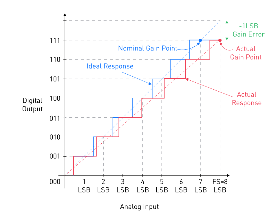
Figure 5: Gain error as the vertical difference between the actual gain point and the straight-line model of an ADC
Impact on ADC Output
The ADC's output scaling is impacted by gain error across the whole input range. Gain error modifies the relationship between input and output proportionality as opposed to offset error, which is a continuous shift. This is particularly significant in applications where relative measurements or accurate amplitude representation are crucial and can result in inaccurate representations of input amplitudes, especially at higher input levels.
Methods for Measuring Gain Error
Understanding and quantifying gain error is essential for compensation and calibration. Here are the common methods:
End-point Method: This approach entails introducing two recognized voltages to the ADC, one at the lower limit of the input range (usually zero) and another at the upper boundary. By gauging the output codes and juxtaposing them with the anticipated values, the gain error can be deduced as the contrast between the factual and anticipated incline of the transfer function.
Best Fit Line Method: Analogous to its application in measuring offset error, the best-fit line method proves valuable in determining gain error as well. By introducing a sequence of known input voltages and configuring a line that best aligns with the output data points, the gradient of this line can be compared with the ideal slope to calculate the gain error.
Code Density Test: In this methodology, a noisy signal is directed to the ADC, and a substantial volume of samples is recorded. The dissemination of output codes can unveil non-linear tendencies, facilitating the calculation of gain error.
Upon quantifying the gain error, it can be rectified through the application of a scaling factor to the ADC's output during the course of signal processing.
Linearity Errors
Linearity is a crucial factor in determining the accuracy and precision of ADCs. The output of an ADC exhibits linearity errors when it deviates from the predicted linear behavior. Differential non-linearity (DNL) and integral non-linearity (INL) are the two basic categories of linearity defects.
Differential Non-Linearity (DNL)
Differential Non-Linearity (DNL) gauges the disparity between the factual step extent of the ADC's transfer function and the anticipated step width. In an ideal ADC, each code width should stand equivalent to 1 Least Significant Bit (LSB). Nonetheless, within practical ADCs, there might be certain fluctuations in the magnitudes of these steps. Consider the depiction of the purple line in Figure 6, which portrays the response of a theoretical ADC where the step sizes lack uniformity. Within this illustration, code 010 showcases a width of 1.25 LSB, while the subsequent code manifests a reduced width of 0.54 LSB. The DNL specification encapsulates the extent to which the ADC steps deviate from the anticipated value.
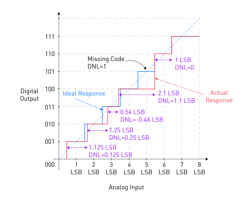
Figure 6: A graph showing the concept of DNL error
DNL can be calculated as follows:
$$DNL(n)=\frac {W(n)-1LSB}{1LSB}$$where Wn denotes width of code n.
As an example, for code 1 (or 001) in Figure 6, we have:
$$DNL(1)=\frac {W(1)-1LSB}{1LSB} = \frac {1.125LSB-1LSB}{1LSB}=0.125$$As a result, code 1's width is 0.125 LSB bigger than it should be. The negative DNL of code 3 (or 011), which has a width of 0.54 LSB, is -0.46 LSB.
A potential "missing code" is indicated by a DNL error of less than or equal to -1, which signifies that some output codes might never be generated by the ADC, regardless of the input. DNL mistakes can skew data and lower the ADC's effective number of bits (ENOB).
Integral Non-Linearity (INL)
Integral Non-Linearity quantifies how far the transfer function of an ADC deviates from a line. A line drawn between the transfer function's endpoints or a best-fit straight line can serve as this line's boundary. INL represents the deviation between the actual transfer function and the desired linear response of the ADC. Think about the transfer curve in Figure 7 as an illustration.
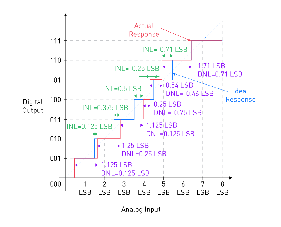
Figure 7: A graph showing the concept of INL error
The differential nonlinearity (DNL) specification describes the departure of a step width from the ideal value. However, because the answer we get depends on how the positive and negative DNL errors are distributed among different codes, the DNL error is unable to adequately characterize the transfer function divergence from the ideal response. We can describe the departure of code transitions from their ideal values using the INL specification. We can use the following equation to determine the INL of code k:
INL of code is characterized by:
$$INL(n)=\frac {T_a(n)-T_{ideal}(n)}{1LSB}$$where Ta(n) and Tideal(n) respectively indicate the optimal and ideal transition from code n-1 to n.
In the previously mentioned instance, the actual shift from code 1 (001) to code 2 (010) takes place at a point that is 0.125 LSB above the ideal transition level. Consequently, the Integral Non-Linearity (INL) of code 2 is calculated as INL(2) = +0.125 LSB.
The INL encompasses cumulative discrepancies and reflects the aggregation of DNL errors up to the nth code. To elaborate, the INL of code 3 corresponds to the summation of the DNL of codes 1 and 2:
$$INL(3)=DNL(1)+DNL(2)=0.125LSB+0.25LSB=0.375LSB$$The concept of INL holds particular significance in situations where the anticipated scenario involves a linear correspondence between the ADC's output codes and the input voltage.
Causes and Impact of Linearity Errors
Causes:
Component Mismatches: DNL and INL faults can be brought on by mismatches in the values of the resistors in resistor ladders or the capacitors in capacitor arrays.
Non-linearities in the Analog Components: Linearity mistakes can be influenced by nonlinearities in the analog components, such as amplifiers and other analog parts of the ADC.
Temperature and Supply Voltage Variations: Variations in temperature and supply voltage can cause component values to drift and hence contribute to linearity problems.
Clock Jitter: When the clock signal fluctuates, the sampling instances fluctuate as well, which can result in linearity issues, particularly at higher frequencies.
Impact:
Harmonic Distortion: The digitized signal may experience harmonic distortion as a result of the ADC's non-linearity.
Reduced Dynamic Range: Linearity faults have the potential to significantly lower the ADC's dynamic range.
Reduction in Resolution: The Effective Number of Bits (ENOB), which is less than the resolution defined by the ADC's bit count, might be reduced as a result of linearity issues.
To assure the linearity of ADCs, particularly in high-precision applications like medical instrumentation, audio processing, and communications, it is imperative to characterize and minimize DNL and INL errors. Among the ways used to lessen the effects of linearity flaws in ADCs include calibration techniques, dithering, and applying oversampling techniques.
Quantization Error
Any Analog-to-Digital Converter's (ADC) inherent limitation is known as quantization error. It has a significant impact on how well an analog signal is represented digitally.
Definition
The finite resolution of an ADC causes quantization error, also known as quantization noise. Only a discrete range of values can be output by an ADC since it represents an analog signal with a limited number of bits. This requires that a set of discrete levels be used to roughly represent the continuous range of the analog input signal. The quantization error is the difference between the real analog value and the closest representable digital value.
If the ADC has a resolution of bits, the quantization error Q can be expressed mathematically as:
$$Q=\frac {V_{max}-V_{min}}{2^n}$$where Vmax and Vmin are the analog input range's maximum and minimum values, respectively.
Impact on Signal Quality
Noise Floor: During the analog-to-digital conversion process, quantization inaccuracy causes quantization noise. It effectively raises the noise floor and reduces the dynamic range of the ADC.
Signal-to-Noise Ratio (SNR): Quantization noise lowers the signal-to-noise ratio (SNR), which is a measure of the signal's strength. The maximal SNR due to quantization noise alone can be estimated for a n-bit ADC using the formula:
$$SNR_{max}[dB]\approx 6.02 \cdot n+1.76$$According to this equation, adding one bit to the ADC's bit depth increases the SNR by around 6 dB.
Harmonic Distortion: Quantization error can cause non-linear harmonic distortion in addition to noise addition to the signal. This is particularly true when the signal's amplitude is small in comparison to the quantization step size. The harmonic content produced by this non-linear distortion may not have been present in the original signal.
Reduction in Effective Resolution: The Effective Number of Bits (ENOB), a measure of the resolution of the ADC, is effectively reduced in the presence of quantization noise. As a result of the noise that quantization error introduces, ENOB is lower than the ADC's real resolution.
There are several methods that can be used to lessen the impact of quantization error, they include oversampling, dithering, or raising the ADC's resolution. These methods can improve the digitized signal's quality and bring it closer to the analog signal's original form. Although quantization error can never be totally removed, it is crucial to understand its implications when designing and using an ADC.
Noise
The inevitability of noise in ADCs might reduce the conversion process' precision and dependability. Understanding noise sources and how they affect ADC performance is crucial.
Thermal Noise
Thermal agitation causes electrons in a conductor to move randomly, creating thermal noise, also known as Johnson-Nyquist noise. Even when there is no signal provided to the ADC, this noise is still present. Since it is a fundamental source of noise, it cannot be completely eradicated, but its impacts can be reduced with the help of effective design methods. Thermal noise's power spectral density is provided by:
$$S=4 \cdot k \cdot T \cdot R$$where R is the resistance in ohms, T is the absolute temperature in kelvin, S is the power spectral density in watts per hertz, and k is the Boltzmann's constant.
One can determine the overall noise voltage over a specific bandwidth (BW) by using:
$$V_{noise}=\sqrt{4 \cdot k \cdot T \cdot R \cdot BW}$$Quantization Noise
The finite resolution of the ADC causes quantization noise, as was previously explained in section 5e. Between the actual analog input and its closest digital approximation, there is noise. The digital values become unclear and inaccurate as a result. Quantization noise, in contrast to thermal noise, is not random but rather depends on a number of variables, one of which being the ADC resolution.
Impact on ADC Performance
Signal-to-Noise Ratio (SNR): The noise floor of the ADC is influenced by both thermal and quantization noise, which influences the SNR. A lower SNR implies that the noise level is higher than the signal, which can result in information loss, especially for signals with tiny amplitudes.
Effective Number of Bits (ENOB): Noise has an impact on the ADC's effective resolution in terms of Effective Number of Bits (ENOB). Noise effectively lowers the amount of bits that may be regarded as accurate, even when an ADC has a high resolution. ENOB is a measurement that takes into account both thermal noise and other noise sources, such as quantization noise.
Dynamic Range: The dynamic range of an ADC, which is the ratio between the largest and smallest signals that can be precisely measured, is constrained by noise. The smallest signal that can be detected above the noise floor has a lower bound determined by noise.
Linearity: Non-linearities can be introduced into the conversion process by noise, particularly quantization noise. This has an impact on the input signal's accurate representation, especially at low amplitudes.
Mitigating Noise Effects
Oversampling: The noise is dispersed over a larger bandwidth by sampling at a rate that is substantially greater than the Nyquist rate, and filtering can then be employed to eliminate the noise outside the intended band.
Averaging: Taking the average of several samples can assist in minimizing the impact of random noise.
Using a Higher Resolution ADC: An ADC with higher resolution will have a smaller quantization step size, which will reduce quantization noise.
Temperature Control: Controlling the operating temperature helps lower thermal noise because thermal noise is temperature-dependent.
Input Signal Conditioning: Signal conditioning techniques, like as filtering, can assist in reducing the amount of noise that reaches the ADC at the input.
Jitter
Jitter pertains to the minor, unintended discrepancies in timing that arise during the sampling moments of an Analog-to-Digital Converter (ADC). These discrepancies can be either haphazard or predictable and can wield a substantial influence on the precision and soundness of the digital rendering of an analog signal, particularly when dealing with high-frequency signals. This section will delve into the explanation and origins of jitter, as well as its repercussions on the accuracy of sampling.
Definition and Causes
Jitter is described as the deviation from the ideal point of sampling. In an ideal ADC setup, sampling instances take place at exact intervals. However, these instances can exhibit minor deviations due to various contributing factors. The fluctuation in the time span between successive sampling moments is denoted as jitter.
Jitter can emerge from several underlying causes:
Noise: Disturbances within the circuit, whether they stem from thermal, shot, or flicker noise, possess the potential to introduce fluctuations into the timing of the clock signal, subsequently resulting in jitter.
Power Supply Fluctuations: Oscillations within the power supply can lead to alterations in the delays of the digital circuits, thereby impacting the timing of the clock signal.
Crosstalk: Unintended electromagnetic interaction between traces on a printed circuit board (PCB) can infuse interference into the clock signal, thus giving rise to jitter.
Phase-Locked Loop (PLL) Instability: When an ADC incorporates a Phase-Locked Loop (PLL) for the purpose of clock generation or synchronization, instability within the PLL mechanism can be a source of jitter.
Temperature Variations: Fluctuations in temperature can wield an influence on the characteristics of the materials within the ADC, ultimately inducing changes in the timing of the clock signal.
Impact on Sampling Accuracy
Harmonic Distortion: Jitter introduces uncertainties into the timing of sampling, which can consequently give rise to harmonic distortion within the digitized signal. This phenomenon becomes particularly conspicuous when dealing with the depiction of components characterized by higher frequencies.
Signal-to-Noise Ratio (SNR) Degradation: The introduction of jitter has a direct effect on the signal-to-noise ratio (SNR) of the digitized signal in that it contributes to noise, leading to a reduction in the SNR. This deterioration in the SNR is especially pronounced when dealing with signals that exhibit high frequencies.
Decrease in Effective Number of Bits (ENOB): The presence of jitter brings about a reduction in the Effective Number of Bits (ENOB) of an ADC. As jitter introduces supplementary noise and distortion, the precision with which the ADC can resolve information diminishes, leading to a lower ENOB.
Errors in Time-Domain Measurements: In scenarios involving time-domain signals, such as applications like digital oscilloscopes, jitter can yield inaccuracies in measurements of time intervals and phase correlations. This can result in errors when trying to quantify these aspects of the signal.
Mitigating the Effects of Jitter
Use of Low-Jitter Clock Sources: Utilizing clock sources with low levels of jitter, such as crystal oscillators, can effectively curtail the inherent jitter present within the ADC.
Proper PCB Design: Adopting meticulous PCB design practices, which encompass factors like adequate shielding and careful trace spacing, can notably diminish both crosstalk and electromagnetic interference. These two factors are significant contributors to the overall jitter in the system.
Supply Filtering: Employing filters along the power supply lines is an effective approach to temper fluctuations in the supply voltage, subsequently leading to a reduction in jitter.
Temperature Stabilization: Establishing temperature stability by operating the ADC within a controlled temperature environment proves instrumental in reducing the jitter that arises from temperature fluctuations.

直接登录
创建新帐号