Introduction and Principle of Operation
The buck-boost converter is a type of DC-DC converter that can produce an output voltage that is either higher or lower than the input voltage, making it a versatile power conversion topology for various applications in power electronics where input voltage regulation and output voltage requirements may vary.
The buck-boost converter operates in two distinct modes: the "buck" mode, where the output voltage is lower than the input voltage, and the "boost" mode, where the output voltage is higher than the input voltage. The transition between these two modes is smooth, enabling the converter to maintain a stable output voltage under varying input conditions.
The buck-boost converter operates using a switch, typically a transistor, and a diode, which control current flow through an inductor and a capacitor. During the switch's ON state, energy is stored in the inductor, and during the OFF state, the energy is transferred to the output through the diode. The duty cycle of the switch, or the ratio of ON time to the total period of the switching cycle, determines the converter's output voltage. Adjusting the duty cycle allows the output voltage to be controlled and maintained at the desired level.
Circuit Topology and Key Components
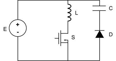
According to the converter's operating theory, magnetic energy obtained from the DC power source E builds up in the inductor over time. This energy is transferred to the load during the time. The voltage at the load must have the polarity depicted in Figure 8 because the diode is positioned in a specific manner. The positive terminal of the load voltage is connected to the negative terminal of the DC power source, indicating that this converter performs voltage inversion at the load. This is an important converter feature that may restrict where it can be used.

Figure 8: The buck-boost converter circuit diagram
When the switch is turned on (Figure 9), the inductor is connected to the DC power source E, causing the inductor current to increase linearly from its minimum to maximum value (Figure 11). During this time, the diode is reverse-biased due to the sum of the voltage across the load U and the DC power source E, and therefore does not conduct.

Figure 9: The buck-boost converter circuit diagram – interval tON
When the switch is turned off, the inductor current is established through the diode D (Figure 10), transferring the magnetic energy of the inductor to the load. Under the influence of the load voltage U, the inductor current decreases from its maximum to minimum value, as shown in Figure 11.

Figure 10: The buck-boost converter circuit diagram – interval tOFF
In steady state, the average value of the voltage across the inductor is zero, which implies:
$$S_+ = E \cdot t_{ON} = S_- = U \cdot t_{OFF} \Rightarrow U = E \cdot \frac{t_{ON}}{t_{OFF}}$$Therefore, this converter can operate as a step-down or step-up converter (tON/tOFF = 0…∞). However, it should be noted that, as with the boost converter, the function of the voltage booster is limited by circuit losses.
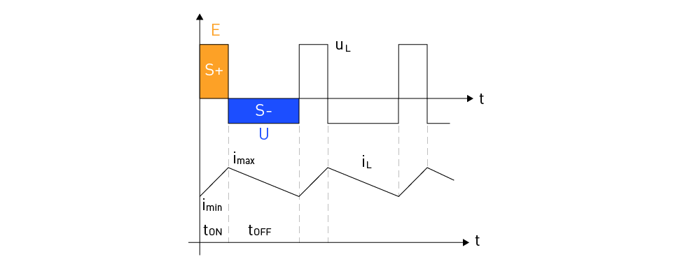
Figure 11: The buck-boost converter – inductor voltage and current versus time graph
The buck-boost converter has some similarities to both the boost converter and the buck converter in its circuit topology. The following are some of the main parts of the buck-boost converter:
Switch (S): Usually, a power transistor, such as a MOSFET, regulates the inductor's current flow. The converter's operating modes and output voltage depend on the switch's ON and OFF states.
Diode (D): When the switch is in the OFF position, it allows current to flow in only one direction, from the inductor to the output. The output capacitor can't discharge back to the input source thanks to the diode.
Inductor (L): Stores energy during the switch's ON state and releases it to the output during the OFF state. The inductor is crucial in smoothing the output voltage and current waveforms.
Capacitor (C): This component filters and smooths the output voltage waveform by storing and releasing energy. It helps maintain a stable output voltage by mitigating voltage ripple and transient responses.
Input and output filters: These are optional components, typically capacitors or inductor-capacitor (LC) combinations, used to reduce electromagnetic interference (EMI) and noise at the input and output of the converter.
The topology of the buck-boost converter can be set up in a variety of ways, including non-inverting, Ćuk, and single-ended primary-inductor converter (SEPIC) configurations. Each of these setups has unique benefits in terms of input-output isolation, voltage polarity, and efficiency.
In conclusion, the buck-boost converter uses critical parts including a switch, diode, inductor, and capacitor to control and sustain the output voltage. It combines the buck and boosts converter topologies. The buck-boost converter's varied configurations provide special benefits that are customized to certain application needs.
Continuous and Discontinuous Conduction Modes
There are two unique conduction modes that buck-boost converters can operate: continuous conduction mode (CCM) and discontinuous conduction mode (DCM). These modes are based on how the inductor current behaves during the switching cycle.
Continuous Conduction Mode (CCM): The inductor current in CCM never reaches zero and always stays positive during the switching cycle. This mode of operation is frequently chosen when a low-output voltage ripple is desired or in high-power applications. Compared to DCM, CCM has superior transient responsiveness, smoother waveforms, and higher efficiency. However, in order to ensure a constant current flow, CCM needs bigger inductor values, which might result in an increase in size and expense.
Discontinuous Conduction Mode (DCM): In DCM, there are periods during the switching cycle when there is no energy transfer to the output because the inductor current falls to zero. When the load current is drastically decreased or in low-power applications, DCM is frequently observed. This method of operation allows for smaller inductor values and a more compact design by streamlining the control strategy. DCM, on the other hand, causes more output voltage ripple, greater switching losses, and less overall efficiency.
The individual application requirements, desired performance traits, and design limitations will determine whether CCM or DCM should be used. A converter might occasionally work in both modes, switching between them when the load current fluctuates. The stability and performance of the system must be maintained in what is known as the border conduction mode (BCM) or critical conduction mode (CrCM), which calls for more complicated control techniques.
Design Considerations and Calculations
Several factors must be considered when designing a buck-boost converter to achieve optimal performance, efficiency, and reliability. These factors include component selection, control strategy, and parameter calculations. This section will provide an overview of the key design considerations and calculations for a buck-boost converter.
Component selection: The performance of the converter is substantially influenced by the choice of many components, including the switching device, diode, inductor, and capacitors. The switching device, usually a MOSFET, needs to be rated for the appropriate voltage and current to withstand the anticipated pressures. The diode should have a low forward voltage drop and a quick reverse recovery time to reduce losses. The inductor should be chosen to sustain either continuous or discontinuous conduction mode as needed and to generate the desired output voltage ripple. To reduce losses, capacitors should have low equivalent series resistance (ESR) and enough capacitance to keep the output voltage stable.
Control strategy: The performance of the transient response, stability maintenance, and output voltage regulation depends greatly on the control strategy. The output voltage is typically managed by pulse-width modulation (PWM), which is frequently used to adjust the duty cycle of the switching device. Under varying load and input voltage conditions, the duty cycle is adjusted by a feedback loop, which commonly makes use of a voltage reference and an error amplifier.
Parameter calculations: Several key parameters must be calculated during the design process to ensure proper operation of the buck-boost converter. These include:
- Duty cycle (D): The duty cycle determines the ratio of the on-time to the total switching period, controlling the output voltage. For a buck-boost converter, the duty cycle can be calculated using the following formula: $$D = \frac{V_{out}}{V_{in} + V_{out}}$$ $$U = E \cdot \frac{ t_{ON}}{t_{OFF}}$$ $$\Rightarrow U + E = U + U \cdot \frac{t_{OFF}}{t_{ON}} = U \cdot \frac{ (t_{ON} + t_{OFF})}{t_{ON}} = U \cdot \frac{ T}{t_{ON}} = \frac{U}{d}$$ $$\Rightarrow d = \frac{U}{U + E} = \frac{V_{out}}{V_{out} + V_{in}}$$
- Inductor value (L): The inductor value affects the output voltage ripple and determines the mode of conduction. The inductor value can be calculated using the desired ripple current (ΔIL), switching frequency (fsw), and the duty cycle (D). In a buck-boost converter, the inductor value can be calculated using the following formula: $$L = \frac{Vin \cdot D}{\Delta I_L \cdot f_{sw}}$$
When the switching device is on (tON), the inductor stores energy and releases it when it is off (tOFF). The difference between the inductor's peak and valley currents during a switching cycle is known as the inductor current ripple (IL). A smaller inductor value will produce a bigger current ripple, which could have an impact on the converter efficiency and output voltage ripple. Depending on the input voltage, duty cycle desired current ripple and switching frequency, a designer can choose the right inductor value to produce the best performance and preserve the application's preferred conduction mode.
Capacitor Values (Cin and Cout): Input and output capacitors help preserve voltage stability and filter out high-frequency noise. Based on the required input and output voltage ripple, switching frequency, and load current, the capacitance values can be calculated. In conclusion, significant thought must be given to component selection, control scheme, and parameter calculations when designing a buck-boost converter. A designer can obtain the best performance, effectiveness, and dependability for the given application by taking these criteria into account.
Efficiency and Losses
Efficiency has a significant impact on the thermal management and overall energy consumption of power converters, making it a crucial performance metric. This section goes over the various elements that affect a buck-boost converter's efficiency and losses.
Conduction losses: The resistance of the converter's parts, particularly the switching mechanism, diode, inductor, and capacitors, causes conduction losses. The switching device's on-state resistance (RDS(on)) and the current passing through it both affect the conduction losses. The forward voltage drop (Vf) and current carried by the diode cause losses in the device. Due to their respective equivalent series resistances (ESR) and DC resistance, the inductor and capacitors sustain losses. Getting rid of these resistances minimizes conduction losses and improves efficiency.
Switching losses: Switching losses happen when a switching device switches between the on and off states. These losses are brought on by the overlapping of voltage and current during transitions and the energy storage in the device's parasitic capacitances. Using devices with low gate charge (Qg) and designing the gate drive circuit to reduce transition times can lower switching losses. Additionally, operating at a lower switching frequency might aid in reducing switching losses, while maintaining output voltage stability and ripple performance can necessitate larger passive components.
Magnetic losses: Hysteresis and eddy currents in the core material, proximity, and skin effects in the winding are all responsible for magnetic losses in inductors. Utilizing suitable core materials with low core losses, improving winding methods, and, in some situations, operating at a lower switching frequency can all help reduce high-frequency magnetic losses.
Control and auxiliary losses: The converter's control circuitry, which includes the gate driver, error amplifier, and voltage reference, also adds to the overall power losses. Even though these losses are often negligible in comparison to the other losses, they should be taken into account when determining the converter's overall efficiency.
Applications and Examples
Buck-boost converters are versatile power conversion devices that find use in a wide range of applications, as they can step up or step down input voltages to meet specific output requirements. This section explores some typical applications and examples of buck-boost converters.
- Portable electronic devices like smartphones, laptops, and medical equipment use batteries that can discharge. Buck-boost converters ensure stable output voltage for optimal performance even when the battery voltage falls below the desired level.
- Energy harvesting systems, such as solar panels and thermoelectric generators, have variable output voltages due to environmental conditions. Buck-boost converters regulate these voltages, providing a stable output for downstream loads or battery charging.
- Automotive electronics have different voltage requirements for various systems, which buck-boost converters can provide by maintaining stable power supplies. This ensures reliable performance, even with varying input voltages due to fluctuations in the vehicle's electrical system or battery voltage.
- Industrial and telecommunications equipment require stable power supplies with tight voltage regulations for proper operation. Buck-boost converters can maintain precise output voltages, even in the presence of input voltage variations caused by line disturbances or load changes.
- Buck-boost converters regulate current and voltage in LED lighting systems, ensuring consistent brightness and extending LED lifespan. These converters can accommodate a wide range of input voltages from different power sources, including batteries, AC-DC adapters, and renewable energy systems.




直接登录
创建新帐号